TL F 5958
CD4027BMCD4027BC
Dual
J-K
MasterSlave
Flip-Flop
with
Set
and
Reset
February 1988
CD4027BM CD4027BC Dual J-K Master Slave
Flip-Flop with Set and Reset
General Description
These dual J-K flip-flops are monolithic complementary
MOS (CMOS) integrated circuits constructed with N- and P-
channel enhancement mode transistors Each flip-flop has
independent J K set reset and clock inputs and buffered
Q and Q outputs These flip-flops are edge sensitive to the
clock input and change state on the positive-going transition
of the clock pulses Set or reset is independent of the clock
and is accomplished by a high level on the respective input
All inputs are protected against damage due to static dis-
charge by diode clamps to V
DD
and V
SS
Features
Y
Wide supply voltage range
3 0V to 15V
Y
High noise immunity
0 45 V
DD
(typ )
Y
Low power TTL
Fan out of 2 driving 74L
compatibility
or 1 driving 74LS
Y
Low power
50 nW (typ )
Y
Medium speed operation
12 MHz (typ )
with 10V supply
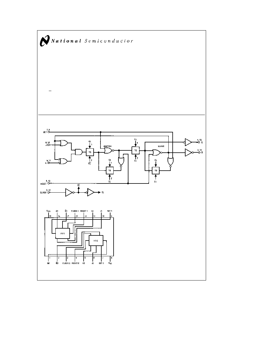
Schematic and Connection Diagrams
TL F 5958 � 1
Dual-In-Line Package
TL F 5958 � 2
Top View
Order Number CD4027B
C1995 National Semiconductor Corporation
RRD-B30M105 Printed in U S A

Absolute Maximum Ratings
(Note 1 and 2)
If Military Aerospace specified devices are required
please contact the National Semiconductor Sales
Office Distributors for availability and specifications
DC Supply Voltage (V
DD
)
b
0 5 V
DC
to
a
18 V
DC
Input Voltage (V
IN
)
b
0 5V to V
DD
a
0 5 V
DC
Storage Temperature Range (T
S
)
b
65 C to
a
150 C
Power Dissipation (P
D
)
Dual-In-Line
700 mW
Small Outline
500 mW
Lead Temperature (T
L
)
(Soldering 10 seconds)
260 C
Recommended Operating
Conditions
(Note 2)
DC Supply Voltage (V
DD
)
3V to 15 V
DC
Input Voltage (V
IN
)
0V to V
DD
V
DC
Operating Temperature Range (T
A
)
CD4027BM
b
55 C to
a
125 C
CD4027BC
b
40 C to
a
85 C
DC Electrical Characteristics
CD4027BM (Note 2)
Symbol
Parameter
Conditions
b
55 C
a
25 C
a
125 C
Units
Min
Max
Min
Typ
Max
Min
Max
I
DD
Quiescent Device Current V
DD
e
5V V
IN
e
V
DD
or V
SS
1
1
30
m
A
V
DD
e
10V V
IN
e
V
DD
or V
SS
2
2
60
m
A
V
DD
e
15V V
IN
e
V
DD
or V
SS
4
4
120
m
A
V
OL
Low Level
l
I
O
l
k
1 mA
Output Voltage
V
DD
e
5V
0 05
0
0 05
0 05
V
V
DD
e
10V
0 05
0
0 05
0 05
V
V
DD
e
15V
0 05
0
0 05
0 05
V
V
OH
High Level
l
I
O
l
k
1 mA
Output Voltage
V
DD
e
5V
4 95
4 95
5
4 95
V
V
DD
e
10V
9 95
9 95
10
9 95
V
V
DD
e
15V
14 95
14 95
15
14 95
V
V
IL
Low Level
V
DD
e
5V V
O
e
0 5V or 4 5V
1 5
1 5
1 5
V
Input Voltage
V
DD
e
10V V
O
e
1V or 9V
3 0
3 0
3 0
V
V
DD
e
15V V
O
e
1 5V or 13 5V
4 0
4 0
4 0
V
V
IH
High Level
V
DD
e
5V V
O
e
0 5V or 4 5V
3 5
3 5
3 5
V
Input Voltage
V
DD
e
10V V
O
e
1V or 9V
7 0
7 0
7 0
V
V
DD
e
15V V
O
e
1 5V or 13 5V
11 0
11 0
11 0
V
I
OL
Low Level Output
V
DD
e
5V V
O
e
0 4V
0 64
0 51
0 88
0 36
mA
Current (Note 3)
V
DD
e
10V V
O
e
0 5V
1 6
1 3
2 25
0 9
mA
V
DD
e
15V V
O
e
1 5V
4 2
3 4
8 8
2 4
mA
I
OH
High Level Output
V
DD
e
5V V
O
e
4 6V
b
0 64
b
0 51
b
0 88
b
0 36
mA
Current (Note 3)
V
DD
e
10V V
O
e
9 5V
b
1 6
b
1 3
b
2 25
b
0 9
mA
V
DD
e
15V V
O
e
13 5V
b
4 2
b
3 4
b
8 8
b
2 4
mA
I
IN
Input Current
V
DD
e
15V V
IN
e
0V
b
0 1
b
10
b
5
b
0 1
b
1 0
m
A
V
DD
e
15V V
IN
e
15V
0 1
10
b
5
0 1
1 0
m
A
Note 1
``Absolute Maximum Ratings'' are those values beyond which the safety of the device cannot be guaranteed They are not meant to imply that the devices
should be operated at these limits The table of ``Recommended Operating Conditions'' and ``Electrical Characteristics'' provides conditions for actual device
operation
Note 2
V
SS
e
0V unless otherwise specified
Note 3
I
OH
and I
OL
are tested one output at a time
2
DC Electrical Characteristics
CD4027BC (Note 2)
Symbol
Parameter
Conditions
b
40 C
a
25 C
a
85 C
Units
Min
Max
Min
Typ
Max
Min
Max
I
DD
Quiescent Device Current V
DD
e
5V V
IN
e
V
DD
or V
SS
4
4
30
m
A
V
DD
e
10V V
IN
e
V
DD
or V
SS
8
8
60
m
A
V
DD
e
15V V
IN
e
V
DD
or V
SS
16
16
120
m
A
V
OL
Low Level
l
I
O
l
k
1 mA
Output Voltage
V
DD
e
5V
0 05
0
0 05
0 05
V
V
DD
e
10V
0 05
0
0 05
0 05
V
V
DD
e
15V
0 05
0
0 05
0 05
V
V
OH
High Level
l
I
O
l
k
1 mA
Output Voltage
V
DD
e
5V
4 95
4 95
5
4 95
V
V
DD
e
10V
9 95
9 95
10
9 95
V
V
DD
e
15V
14 95
14 95
15
14 95
V
V
IL
Low Level
V
DD
e
5V V
O
e
0 5V or 4 5V
1 5
1 5
1 5
V
Input Voltage
V
DD
e
10V V
O
e
1V or 9V
3 0
3 0
3 0
V
V
DD
e
15V V
O
e
1 5V or 13 5V
4 0
4 0
4 0
V
V
IH
High Level
V
DD
e
5V V
O
e
0 5V or 4 5V
3 5
3 5
3 5
V
Input Voltage
V
DD
e
10V V
O
e
1V or 9V
7 0
7 0
7 0
V
V
DD
e
15V V
O
e
1 5V or 13 5V
11 0
11 0
11 0
V
I
OL
Low Level Output
V
DD
e
5V V
O
e
0 4V
0 52
0 44
0 88
0 36
mA
Current (Note 3)
V
DD
e
10V V
O
e
0 5V
1 3
1 1
2 25
0 9
mA
V
DD
e
15V V
O
e
1 5V
3 6
3 0
8 8
2 4
mA
I
OH
High Level Output
V
DD
e
5V V
O
e
4 6V
b
0 52
b
0 44
b
0 88
b
0 36
mA
Current (Note 3)
V
DD
e
10V V
O
e
9 5V
b
1 3
b
1 1
b
2 25
b
0 9
mA
V
DD
e
15V V
O
e
13 5V
b
3 6
b
3 0
b
8 8
b
2 4
mA
I
IN
Input Current
V
DD
e
15V V
IN
e
0V
b
0 3
b
10
b
5
b
0 3
b
1 0
m
A
V
DD
e
15V V
IN
e
15V
0 3
10
b
5
0 3
1 0
m
A
Note 1
``Absolute Maximum Ratings'' are those values beyond which the safety of the device cannot be guaranteed They are not meant to imply that the devices
should be operated at these limits The table of ``Recommended Operating Conditions'' and ``Electrical Characteristics'' provides conditions for actual device
operation
Note 2
V
SS
e
0V unless otherwise specified
Note 3
I
OH
and I
OL
are tested one output at a time
3

AC Electrical Characteristics
T
A
e
25 C C
L
e
50 pF t
rCL
e
t
fCL
e
20 ns unless otherwise specified
Symbol
Parameter
Conditions
Min
Typ
Max
Units
t
PHL
or t
PLH
Propagation Delay Time
V
DD
e
5V
200
400
ns
from Clock to Q or Q
V
DD
e
10V
80
160
ns
V
DD
e
15V
65
130
ns
t
PHL
or t
PLH
Propagation Delay Time
V
DD
e
5V
170
340
ns
from Set to Q or Reset to Q
V
DD
e
10V
70
140
ns
V
DD
e
15V
55
110
ns
t
PHL
or t
PLH
Propagation Delay Time
V
DD
e
5V
110
220
ns
from Set to Q or
V
DD
e
10V
50
100
ns
Reset to Q
V
DD
e
15V
40
80
ns
t
S
Minimum Data Setup Time
V
DD
e
5V
135
270
ns
V
DD
e
10V
55
110
ns
V
DD
e
15V
45
90
ns
t
THL
or t
TLH
Transition Time
V
DD
e
5V
100
200
ns
V
DD
e
10V
50
100
ns
V
DD
e
15V
40
80
ns
f
CL
Maximum Clock Frequency
V
DD
e
5V
2 5
5
MHz
(Toggle Mode)
V
DD
e
10V
6 2
12 5
MHz
V
DD
e
15V
7 6
15 5
MHz
t
rCL
or t
fCL
Maximum Clock Rise
V
DD
e
5V
15
m
s
and Fall Time
V
DD
e
10V
10
m
s
V
DD
e
15V
5
m
s
t
W
Minimum Clock Pulse
V
DD
e
5V
100
200
ns
Width (t
WH
e
t
WL
)
V
DD
e
10V
40
80
ns
V
DD
e
15V
32
65
ns
t
WH
Minimum Set and
V
DD
e
5V
80
160
ns
Reset Pulse Width
V
DD
e
10V
30
60
ns
V
DD
e
15V
25
50
ns
C
IN
Average Input Capacitance
Any Input
5
7 5
pF
C
PD
Power Dissipation Capacity
Per Flip-Flop
35
pF
(Note 4)
AC Parameters are guaranteed by DC correlated testing
Note 1
``Absolute Maximum Ratings'' are those values beyond which the safety of the device cannot be guaranteed They are not meant to imply that the
devices should be operated at these limits The table of ``Recommended Operating Conditions'' and ``Electrical Characteristics'' provides conditions for actual
device operation
Note 2
V
SS
e
0V unless otherwise specified
Note 3
I
OH
and I
OL
are tested one output at a time
Note 4
C
PD
determines the no load AC power consumption of any CMOS device For complete explanation see 54C 74C Family Characteristics application
note AN-90
4

Typical Applications
Ripple Binary Counters
TL F 5958 � 3
Shift Registers
TL F 5958 � 4
Truth Table
tnb1
Inputs
X
tn
Outputs
CL
U
J
K
S
R
Q
Q
Q
L
I
X
O
O
O
I
O
L
X
O
O
O
I
I
O
L
O
X
O
O
O
O
I
L
X
I
O
O
I
O
I
K
X
X
O
O
X
(No Change)
X
X
X
I
O
X
I
O
X
X
X
O
I
X
O
I
X
X
X
I
I
X
I
I
Where
I
e
High Level
O
e
Low Level
U e
Level Change
X
e
Don't Care
e
t
n
b
1
refers to the time interval prior to the positive clock pulse transition
X e
t
n
refers to the time intervals after the positive clock pulse transition
5