 | –≠–ª–µ–∫—Ç—Ä–æ–Ω–Ω—ã–π –∫–æ–º–ø–æ–Ω–µ–Ω—Ç: 4069UB | –°–∫–∞—á–∞—Ç—å:  PDF PDF  ZIP ZIP |

TL F 5975
CD4069UBMCD4069UBC
Inverter
Circuits
February 1988
CD4069UBM CD4069UBC Inverter Circuits
General Description
The CD4069UB consists of six inverter circuits and is manu-
factured using complementary MOS (CMOS) to achieve
wide power supply operating range low power consump-
tion high noise immunity and symmetric controlled rise and
fall times
This device is intended for all general purpose inverter appli-
cations where the special characteristics of the MM74C901
MM74C903 MM74C907 and CD4049A Hex Inverter Buff-
ers are not required In those applications requiring larger
noise immunity the MM74C14 or MM74C914 Hex Schmitt
Trigger is suggested
All inputs are protected from damage due to static dis-
charge by diode clamps to V
DD
and V
SS
Features
Y
Wide supply voltage range
3 0V to 15V
Y
High noise immunity
0 45 V
DD
typ
Y
Low power TTL
Fan out of 2 driving 74L
compatibility
or 1 driving 74LS
Y
Equivalent to MM54C04 MM74C04
Schematic and Connection Diagram
TL F 5975 ≠ 1
Dual-In-Line Package
TL F 5975 ≠ 2
Order Number CD4069UB
AC Test Circuits and Switching Time Waveforms
TL F 5975 ≠ 3
TL F 5975 ≠ 4
C1995 National Semiconductor Corporation
RRD-B30M105 Printed in U S A

Absolute Maximum Ratings
(Notes 1
2)
If Military Aerospace specified devices are required
please contact the National Semiconductor Sales
Office Distributors for availability and specifications
DC Supply Voltage (V
DD
)
b
0 5V to
a
18 V
DC
Input Voltage (V
IN
)
b
0 5V to V
DD
a
0 5 V
DC
Storage Temperature Range (T
S
)
b
65 C to
a
150 C
Power Dissipation (P
D
)
Dual-In-Line
700 mW
Small Outline
500 mW
Lead Temperature (T
L
)
(Soldering 10 seconds)
260 C
Recommended Operating
Conditions
(Note 2)
DC Supply Voltage (V
DD
)
3V to 15V
DC
Input Voltage (V
IN
)
0V to V
DD
V
DC
Operating Temperature Range (T
A
)
CD4069UBM
b
55 C to
a
125 C
CD4069UBC
b
40 C to
a
85 C
DC Electrical Characteristics
CD4069UBM (Note 2)
Symbol
Parameter
Conditions
b
55 C
a
25 C
a
125 C
Units
Min
Max
Min
Typ
Max
Min
Max
I
DD
Quiescent Device Current
V
DD
e
5V
0 25
0 25
7 5
m
A
V
IN
e
V
DD
or V
SS
V
DD
e
10V
0 5
0 5
15
m
A
V
IN
e
V
DD
or V
SS
V
DD
e
15V
1 0
1 0
30
m
A
V
IN
e
V
DD
or V
SS
V
OL
Low Level Output Voltage
l
I
O
l
k
1 mA
V
DD
e
5V
0 05
0
0 05
0 05
V
V
DD
e
10V
0 05
0
0 05
0 05
V
V
DD
e
15V
0 05
0
0 05
0 05
V
V
OH
High Level Output Voltage
l
I
O
l
k
1 mA
V
DD
e
5V
4 95
4 95
5
4 95
V
V
DD
e
10V
9 95
9 95
10
9 95
V
V
DD
e
15V
14 95
14 95
15
14 95
V
V
IL
Low Level Input Voltage
l
I
O
l
k
1 mA
V
DD
e
5V V
O
e
4 5V
1 0
1 0
1 0
V
V
DD
e
10V V
O
e
9V
2 0
2 0
2 0
V
V
DD
e
15V V
O
e
13 5V
3 0
3 0
3 0
V
V
IH
High Level Input Voltage
l
I
O
l
k
1 mA
V
DD
e
5V V
O
e
0 5V
4 0
4 0
4 0
V
V
DD
e
10V V
O
e
1V
8 0
8 0
8 0
V
V
DD
e
15V V
O
e
1 5V
12 0
12 0
12 0
V
I
OL
Low Level Output Current
V
DD
e
5V V
O
e
0 4V
0 64
0 51
0 88
0 36
mA
(Note 3)
V
DD
e
10V V
O
e
0 5V
1 6
1 3
2 25
0 9
mA
V
DD
e
15V V
O
e
1 5V
4 2
3 4
8 8
2 4
mA
I
OH
High Level Output Current
V
DD
e
5V V
O
e
4 6V
b
0 64
b
0 51
b
0 88
b
0 36
mA
(Note 3)
V
DD
e
10V V
O
e
9 5V
b
1 6
b
1 3
b
2 25
b
0 9
mA
V
DD
e
15V V
O
e
13 5V
b
4 2
b
3 4
b
8 8
b
2 4
mA
I
IN
Input Current
V
DD
e
15V V
IN
e
0V
b
0 10
b
10
b
5
b
0 10
b
1 0
m
A
V
DD
e
15V V
IN
e
15V
0 10
10
b
5
0 10
1 0
m
A
Note 1
``Absolute Maximum Ratings'' are those values beyond which the safety of the device cannot be guaranteed They are not meant to imply that the devices
should be operated at these limits The table of ``Recommended Operating Conditions'' and ``Electrical Characteristics'' provides conditions for actual device
operation
Note 2
V
SS
e
0V unless otherwise specified
Note 3
I
OH
and I
OL
are tested one output at a time
2

DC Electrical Characteristics
CD4069UBC (Note 2)
Symbol
Parameter
Conditions
b
40 C
a
25 C
a
85 C
Units
Min
Max
Min
Typ
Max
Min
Max
I
DD
Quiescent Device Current
V
DD
e
5V
1 0
1 0
7 5
m
A
V
IN
e
V
DD
or V
SS
V
DD
e
10V
2 0
2 0
15
m
A
V
IN
e
V
DD
or V
SS
V
DD
e
15V
4 0
4 0
30
m
A
V
IN
e
V
DD
or V
SS
V
OL
Low Level Output Voltage
l
I
O
l
k
1 mA
V
DD
e
5V
0 05
0
0 05
0 05
V
V
DD
e
10V
0 05
0
0 05
0 05
V
V
DD
e
15V
0 05
0
0 05
0 05
V
V
OH
High Level Output Voltage
l
I
O
l
k
1 mA
V
DD
e
5V
4 95
4 95
4 95
V
V
DD
e
10V
9 95
9 95
9 95
V
V
DD
e
15V
14 95
14 95
14 95
V
V
IL
Low Level Input Voltage
l
I
O
l
k
1 mA
V
DD
e
5V V
O
e
4 5V
1 0
1 0
1 0
V
V
DD
e
10V V
O
e
9V
2 0
2 0
2 0
V
V
DD
e
15V V
O
e
13 5V
3 0
3 0
3 0
V
V
IH
High Level Input Voltage
l
I
O
l
k
1 mA
V
DD
e
5V V
O
e
0 5V
4 0
4 0
4 0
V
V
DD
e
10V V
O
e
1V
8 0
8 0
8 0
V
V
DD
e
15V V
O
e
1 5V
12 0
12 0
12 0
V
I
OL
Low Level Output Current
V
DD
e
5V V
O
e
0 4V
0 52
0 44
0 88
0 36
mA
(Note 3)
V
DD
e
10V V
O
e
0 5V
1 3
1 1
2 25
0 9
mA
V
DD
e
15V V
O
e
1 5V
3 6
3 0
8 8
2 4
mA
I
OH
High Level Output Current
V
DD
e
5V V
O
e
4 6V
b
0 52
b
0 44
b
0 88
b
0 36
mA
(Note 3)
V
DD
e
10V V
O
e
9 5V
b
1 3
b
1 1
b
2 25
b
0 9
mA
V
DD
e
15V V
O
e
13 5V
b
3 6
b
3 0
b
8 8
b
2 4
mA
I
IN
Input Current
V
DD
e
15V V
IN
e
0V
b
0 30
b
10
b
5
b
0 30
b
1 0
m
A
V
DD
e
15V V
IN
e
15V
0 30
10
b
5
0 30
1 0
m
A
AC Electrical Characteristics
T
A
e
25 C C
L
e
50 pF R
L
e
200 kX t
r
and t
f
s
20 ns unless otherwise specified
Symbol
Parameter
Conditions
Min
Typ
Max
Units
t
PHL
or t
PLH
Propagation Delay Time from
V
DD
e
5V
50
90
ns
Input to Output
V
DD
e
10V
30
60
ns
V
DD
e
15V
25
50
ns
t
THL
or t
TLH
Transition Time
V
DD
e
5V
80
150
ns
V
DD
e
10V
50
100
ns
V
DD
e
15V
40
80
ns
C
IN
Average Input Capacitance
Any Gate
6
15
pF
C
PD
Power Dissipation Capacitance
Any Gate (Note 4)
12
pF
AC Parameters are guaranteed by DC correlated testing
Note 1
``Absolute Maximum Ratings'' are those values beyond which the safety of the device cannot be guaranteed They are not meant to imply that the devices
should be operated at these limits The table of ``Recommended Operating Conditions'' and ``Electrical Characteristics'' provides conditions for actual device
operation
Note 2
V
SS
e
0V unless otherwise specified
Note 3
I
OH
and I
OL
are tested one output at a time
Note 4
C
PD
determines the no load AC power consumption of any CMOS device For complete explanation see 54C 74C Family Characteristics application
note
AN-90
3
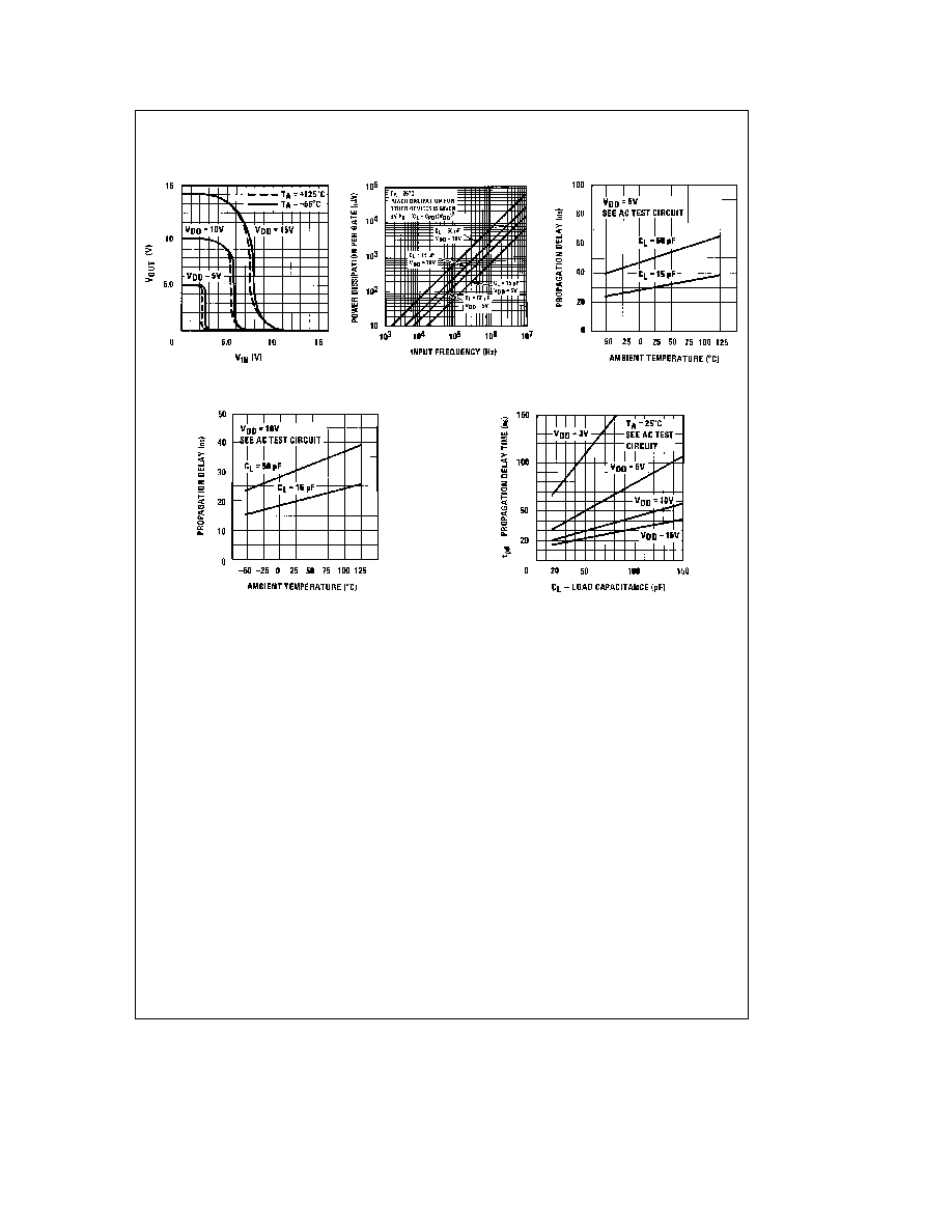
Typical Performance Characteristics
Gate Transfer Characteristics
TL F 5975 ≠ 5
Power Dissipation vs
Frequency
TL F 5975 ≠ 6
Propagation Delay vs
Ambient Temperature
TL F 5975 ≠ 7
Propagation Delay vs
Ambient Temperature
TL F 5975 ≠ 8
Propagation Delay Time
vs Load Capacitance
TL F 5975 ≠ 9
4

Physical Dimensions
inches (millimeters)
Ceramic Dual-In-Line Package (J)
Order Number CD4069UBMJ or CD4069UBCJ
NS Package Number J14A
5