 | –≠–ª–µ–∫—Ç—Ä–æ–Ω–Ω—ã–π –∫–æ–º–ø–æ–Ω–µ–Ω—Ç: 52F2278 | –°–∫–∞—á–∞—Ç—å:  PDF PDF  ZIP ZIP |
©
Semiconductor Components Industries, LLC, 2000
April, 2000 ≠ Rev. 8
1
Publication Order Number:
MC33269/D
MC33269
Low Dropout Positive Fixed
and Adjustable Voltage
Regulators
The MC33269 series are low dropout, medium current, fixed and
adjustable, positive voltage regulators specifically designed for use in
low input voltage applications. These devices offer the circuit designer
an economical solution for precision voltage regulation, while keeping
power losses to a minimum.
The regulator consists of a 1.0 V dropout composite PNP≠NPN pass
transistor, current limiting, and thermal shutdown.
∑
3.3 V, 5.0 V, 12 V and Adjustable Versions.
2.85 V version available as MC34268.
∑
Space Saving DPAK, SOP≠8 and SOT≠223 Power Packages
∑
1.0 V Dropout
∑
Output Current in Excess of 800 mA
∑
Thermal Protection
∑
Short Circuit Protection
∑
Output Trimmed to 1.0% Tolerance
DEVICE TYPE / NOMINAL OUTPUT VOLTAGE
MC33269D
Adj
MC33269D≠5.0
5.0 V
MC33269DT
Adj
MC33269DT≠5.0
5.0 V
MC33269T
Adj
MC33269T≠5.0
5.0 V
MC33269D≠3.3
3.3 V
MC33269D≠12
12 V
MC33269DT≠3.3
3.3 V
MC33269DT≠12
12 V
MC33269T≠3.3
3.3 V
MC33269T≠12
12 V
MC33269ST≠3.3
3.3 V
TO≠220AB
T SUFFIX
CASE 221A
http://onsemi.com
See detailed ordering and shipping information in the package
dimensions section on page 7 of this data sheet.
ORDERING INFORMATION
8
1
8
7
6
5
1
2
3
4
Gnd/Adj
SOP≠8
D SUFFIX
CASE 751
DPAK
DT SUFFIX
CASE 369A
Vin
NC
NC
1. Gnd/Adj
1
2
3
2. Vout
3. Vin
(Top View)
(Top View)
1
3
Vout
Vout
Heatsink surface (shown as terminal 4 in
case outline drawing) is connected to Pin 2.
Heatsink surface (shown as terminal 4 in
case outline drawing) is connected to Pin 2.
Pin: 1. Gnd/Adj
2. Vout
3. Vin
3
1
2
1 2 3
(Top View)
SOT≠223
ST SUFFIX
CASE 318E
1
3
MC33269
http://onsemi.com
2
MAXIMUM RATINGS
Rating
Symbol
Value
Unit
Power Supply Input Voltage
Vin
20
V
Power Dissipation
Case 369A (DPAK)
TA = 25
∞
C
PD
Internally Limited
W
Thermal Resistance, Junction≠to≠Ambient
JA
92
∞
C/W
Thermal Resistance, Junction≠to≠Case
JC
6.0
∞
C/W
Case 751 (SOP≠8)
TA = 25
∞
C
PD
Internally Limited
W
Thermal Resistance, Junction≠to≠Ambient
JA
160
∞
C/W
Thermal Resistance, Junction≠to≠Case
JC
25
∞
C/W
Case 221A
TA = 25
∞
C
PD
Internally Limited
W
Thermal Resistance, Junction≠to≠Ambient
JA
65
∞
C/W
Thermal Resistance, Junction≠to≠Case
JC
5.0
∞
C/W
Case 318E
TA = 25
∞
C
PD
Internally Limited
W
Thermal Resistance, Junction≠to≠Ambient
JA
245
∞
C/W
Thermal Resistance, Junction≠to≠Case
JC
15
∞
C/W
Operating Junction Temperature Range
TJ
≠40 to +150
∞
C
Storage Temperature
Tstg
≠55 to +150
∞
C
NOTE: ESD data available upon request.
ELECTRICAL CHARACTERISTICS
(CO = 10
µ
F, TA = 25
∞
C, for min/max values TJ = ≠40
∞
C to +125
∞
C, unless otherwise noted.)
Characteristic
Symbol
Min
Typ
Max
Unit
Output Voltage (Iout = 10 mA, TJ = 25
∞
C)
VO
V
3.3 Suffix (VCC = 5.3 V)
3.27
3.3
3.33
5.0 Suffix (VCC = 7.0 V)
4.95
5.0
5.05
12 Suffix (VCC = 14 V)
11.88
12
12.12
Output Voltage (Line, Load and Temperature) (Note 1.)
VO
V
(1.25 V
Vin ≠ Vout
15 V, Iout = 500 mA)
(1.35 V
Vin ≠ Vout
10 V, Iout = 800 mA)
3.3 Suffix
3.23
3.3
3.37
5.0 Suffix
4.9
5.0
5.1
12 Suffix
11.76
12
12.24
Reference Voltage (Iout = 10 mA, Vin ≠ Vout = 2.0 V, TJ = 25
∞
C)
Vref
1.235
1.25
1.265
V
for Adjustable Voltage
Reference Voltage (Line, Load and Temperature) (Note 1.)
Vref
1.225
1.25
1.275
V
(1.25 V
Vin ≠ Vout
15 V, Iout = 500 mA)
(1.35 V
Vin ≠ Vout
10 V, Iout = 800 mA)
for Adjustable Voltage
Line Regulation
Regline
≠
≠
0.3
%
(Iout = 10 mA, Vin = [Vout + 1.5 V] to Vin = 20 V, TJ = 25
∞
C)
Load Regulation (Vin = Vout + 3.0 V, Iout = 10 mA to 800 mA, TJ = 25
∞
C)
Regload
≠
≠
0.5
%
Dropout Voltage
Vin ≠ Vout
V
(Iout = 500 mA)
≠
1.0
1.25
(Iout = 800 mA)
≠
1.1
1.35
Ripple Rejection
RR
55
≠
≠
dB
(10 Vpp, 120 Hz Sinewave; Iout = 500 mA)
Current Limit (Vin ≠ Vout = 10 V)
ILimit
800
≠
≠
mA
Quiescent Current (Fixed Output)
(1.5 V
Vout
3.3 V)
(5 V
Vout
12 V)
IQ
≠
≠
5.5
≠
8.0
20
mA
1. The MC33269≠12, Vin ≠ Vout is limited to 8.0 V maximum, because of the 20 V maximum rating applied to Vin.

MC33269
http://onsemi.com
3
ELECTRICAL CHARACTERISTICS
(CO = 10
µ
F, TA = 25
∞
C, for min/max values TJ = ≠40
∞
C to +125
∞
C, unless otherwise noted.)
Characteristic
Symbol
Min
Typ
Max
Unit
Minimum Required Load Current
ILoad
mA
Fixed Output Voltage
≠
≠
0
Adjustable Voltage
8.0
≠
≠
Adjustment Pin Current
IAdj
≠
≠
120
µ
A
Vin
Vout
VAdj
Gnd
Trim Links
Internal Schematic
This device contains 38 active transistors.

MC33269
http://onsemi.com
4
IO, OUTPUT LOAD CURRENT (mA)
in
V
out
≠V
Figure 1. Dropout Voltage versus
Output Load Current
1.5
1.3
1.1
0.9
0.7
0.5
0
200
400
600
800
1000
Figure 2. Transient Load Regulation
,
DR
O
P
O
U
T
VOL
T
A
G
E
(V)
20 ms/DIV
Cin = 10
µ
F
CO = 10
µ
F Tantalum
Vin = VO + 3.0 V
Preload = 0.1 A
0 A
0.5 A
100
, OUTPUT
I O
V
O
, OUTPUT
VOL
T
AGE DEVIA
TION
CURRENT
TA = 25
∞
C
TA = ≠40
∞
C
TA = 125
∞
C
mV/Div
≠55
900
≠25
0
25
50
75
100
125
940
980
1020
1060
1100
Figure 3. Dropout Voltage
versus Temperature
Figure 4. MC33269≠XX Output DC Current versus
Input≠Output Differential Voltage
V
TA, AMBIENT TEMPERATURE (
∞
C)
IO = 800 mA
,
OV
ER
VOL
T
A
G
E
IN
PU
T
T
HRESH
OL
D
(
%
V
)
FB(OV)
FB
0
0.2
0.4
0.6
0.8
1.0
1.2
1.4
1.6
0
2.0
4.0
6.0
8.0
10
12
14
16
INPUT≠OUTPUT VOLTAGE DIFFERENTIAL (V)
TA = 25
∞
C
MC33269D≠XX
L = 25 mm Copper
OUTPUT
CURRENT
(A)
70
0.1
1.0
10
100
60
50
40
30
20
Figure 5. MC33269 Ripple Rejection
versus Frequency
Figure 6. MC33269≠ADJ Ripple Rejection
versus Frequency
RR
,
R
I
PP
L
E REJE
CTION
R
A
TIO
(d
B
)
f, FREQUENCY (kHz)
20
30
40
50
60
70
RR, RIPPLE REJECTION RA
TIO (dB)
100
10
1.0
f, FREQUENCY (kHz)
Vin = 8.0 V
Vout = 5.0 V
IL = 800 mA
CAdj = 22
µ
F
TA = 25
∞
C
0.1
Vin = VO + 3.0 V
IL = 800 mA
TA = 25
∞
C
VO = 12 V
VO = 3.3 V or 5.0 V
MC33269
http://onsemi.com
5
œœœ
œœœ
œœœ
R
,
THERMAL
RESIST
ANCE
JA
JUNCTION-T
O-AIR ( C/W)
∞
40
80
120
160
200
240
280
0.35
0.42
0.50
0.63
0.83
1.25
2.50
0
10
20
30
25
15
5.0
L, LENGTH OF COPPER (mm)
PD(max) for TA = 50
∞
C
Minimum
Size Pad
P
D
L
L
, MAXIMUM POWER DISSIP
A
TION (W)
Free Air
Mounted
Vertically
R
JA
2.0 oz. Copper
œœœœ
œœœœ
œœœœ
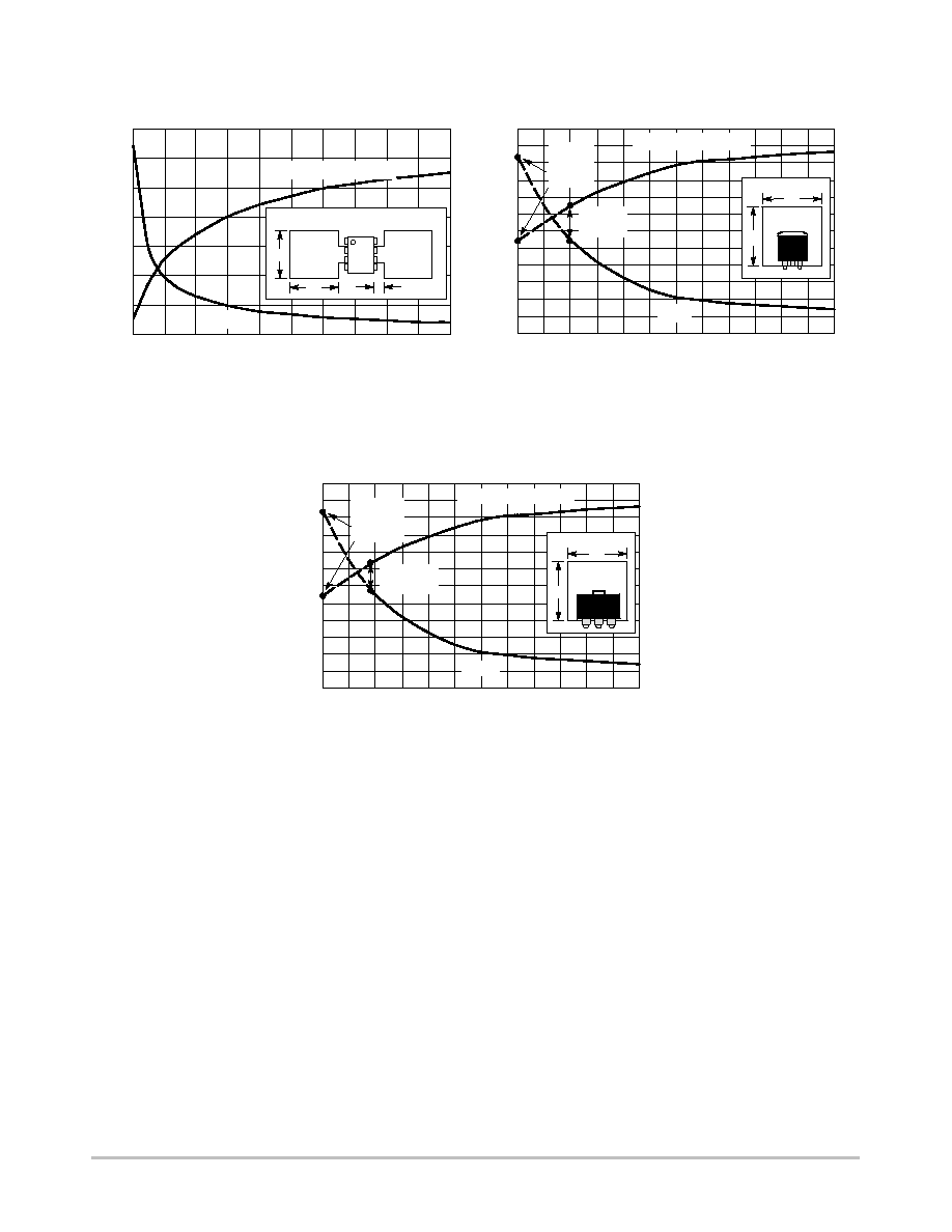
Figure 7. SOP≠8 Thermal Resistance and Maximum
Power Dissipation versus P.C.B. Copper Length
R
,
T
HERM
AL
RES
I
S
T
ANC
E
,
JA
JU
NCTION≠T
O≠AI
R
(
C/
W
)
∞
R
JA
œœœ
œœœ
œœœ
œœœ
œœœ
2.0 oz.
Copper
Graph represents symmetrical layout
3.0 mm
L
L
PD(max) for TA = 50
∞
C
30
50
70
90
110
130
150
170
L, LENGTH OF COPPER (mm)
0
20
30
50
40
10
0.4
0.8
1.2
1.6
2.0
2.4
2.8
3.2
R
,
THERMAL
RESIST
ANCE,
JA
JUNCTION≠T
O≠AIR ( C/W)
∞
Figure 8. DPAK Thermal Resistance and Maximum
Power Dissipation versus P.C.B. Copper Length
L
œœœœ
œœœœ
œœœœ
œœœœ
2.0 oz. Copper
R
JA
Minimum
Size Pad
Free Air
Mounted
Vertically
PD(max) for TA = 50
∞
C
L
40
50
60
70
80
90
100
0
10
20
30
25
15
5.0
L, LENGTH OF COPPER (mm)
0
0.4
0.8
1.2
1.6
2.0
2.4
Figure 9. SOT≠223 Thermal Resistance and Maximum
Power Dissipation versus P.C.B. Copper Length