 | –≠–ª–µ–∫—Ç—Ä–æ–Ω–Ω—ã–π –∫–æ–º–ø–æ–Ω–µ–Ω—Ç: 54125DMQB | –°–∫–∞—á–∞—Ç—å:  PDF PDF  ZIP ZIP |
TL F 6540
54125DM54125DM74125
Quad
TRI-STATE
Buffers
June 1989
54125 DM54125 DM74125
Quad TRI-STATE
Buffers
General Description
This device contains four independent gates each of which
performs a non-inverting buffer function The outputs have
the TRI-STATE feature When enabled the outputs exhibit
the low impedance characteristics of a standard TTL output
with additional drive capability at the high Logic level to per-
mit the driving of bus lines without external pull-up resistors
When disabled both the output transistors are turned off
presenting a high-impedance state to the bus line Thus the
output will act neither as a significant load nor as a driver
To minimize the possibility that two outputs will attempt to
take a common bus to opposite logic levels the disable time
is shorter than the enable time of the outputs
Features
Y
Alternate Military Aerospace device (54125) is avail-
able Contact a National Semiconductor Sales Office
Distributor for specifications
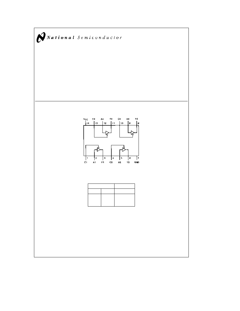
Connection Diagram
Dual-In-Line Package
TL F 6540 ≠ 1
Order Number 54125DMQB 54125FMQB DM54125J DM54125W or DM74125N
See NS Package Number J14A N14A or W14B
Function Table
Y
e
A
Inputs
Output
A
C
Y
L
L
L
H
L
H
X
H
Hi-Z
H
e
High Logic Level
L
e
Low Logic Level
X
e
Either Low or High Logic Level
Hi-Z
e
TRI-STATE (Outputs are disabled)
TRI-STATE
is a registered trademark of National Semiconductor Corporation
C1995 National Semiconductor Corporation
RRD-B30M105 Printed in U S A
Absolute Maximum Ratings
(Note)
If Military Aerospace specified devices are required
please contact the National Semiconductor Sales
Office Distributors for availability and specifications
Supply Voltage
7V
Input Voltage
5 5V
Operating Free Air Temperature Range
DM54 and 54
b
55 C to
a
125 C
DM74
0 C to
a
70 C
Storage Temperature Range
b
65 C to
a
150 C
Note
The ``Absolute Maximum Ratings'' are those values
beyond which the safety of the device cannot be guaran-
teed The device should not be operated at these limits The
parametric values defined in the ``Electrical Characteristics''
table are not guaranteed at the absolute maximum ratings
The ``Recommended Operating Conditions'' table will define
the conditions for actual device operation
Recommended Operating Conditions
Symbol
Parameter
DM54125
DM74125
Units
Min
Nom
Max
Min
Nom
Max
V
CC
Supply Voltage
4 5
5
5 5
4 75
5
5 25
V
V
IH
High Level Input Voltage
2
2
V
V
IL
Low Level Input Voltage
0 8
0 8
V
I
OH
High Level Output Current
b
2
b
5 2
mA
I
OL
Low Level Output Current
16
16
mA
T
A
Free Air Operating Temperature
b
55
125
0
70
C
Electrical Characteristics
over recommended operating free air temperature range (unless otherwise noted)
Symbol
Parameter
Conditions
Min
Typ
Max
Units
(Note 1)
V
I
Input Clamp Voltage
V
CC
e
Min I
I
e b
12 mA
b
1 5
V
V
OH
High Level Output
V
CC
e
Min I
OH
e
Max
2 4
3 3
V
Voltage
V
IL
e
Max V
IH
e
Min
V
OL
Low Level Output
V
CC
e
Min I
OL
e
Max
0 2
0 4
V
Voltage
V
IH
e
Min V
IL
e
Max
I
I
Input Current
Max
V
CC
e
Max V
I
e
5 5V
1
mA
Input Voltage
I
IH
High Level Input Current
V
CC
e
Max V
I
e
2 4V
40
m
A
I
IL
Low Level Input Current
V
CC
e
Max V
I
e
0 4V
b
1 6
mA
I
IZL
Off-State Input Current
V
CC
e
Max V
I
e
0 4V
with Low Level Input
b
40
m
A
Voltage Applied
I
OZH
Off-State Output Current
V
CC
e
Max V
O
e
2 4V
with High Level Output
V
IH
e
Min V
IL
e
Max
40
m
A
Voltage Applied
I
OZL
Off-State Output Current
V
CC
e
Max V
O
e
0 4V
with Low Level Output
V
IH
e
Min V
IL
e
Max
b
40
m
A
Voltage Applied
I
OS
Short Circuit
V
CC
e
Max
DM54
b
30
b
70
mA
Output Current
(Note 2)
DM74
b
28
b
70
I
CC
Supply Current
V
CC
e
Max (Note 3)
36
54
mA
Note 1
All typicals are at V
CC
e
5V T
A
e
25 C
Note 2
Not more than one output should be shorted at a time
Note 3
I
CC
is measured with the output control (C) inputs at 4 5V the data inputs grounded and the outputs open
2
Switching Characteristics
at V
CC
e
5V and T
A
e
25 C (See Section 1 for Test Waveforms and Output Load)
R
L
e
400X
Symbol
Parameter
C
L
e
5 pF
C
L
e
50 pF
Units
Min
Max
Min
Max
t
PLH
Propagation Delay Time
15
ns
Low to High Level Output
t
PHL
Propagation Delay Time
18
ns
High to Low Level Output
t
PZH
Output Enable Time to
18
ns
High Level Output
t
PZL
Output Enable Time to
25
ns
Low Level Output
t
PHZ
Output Disable Time from
8
ns
High Level Output
t
PLZ
Output Disable Time from
14
ns
Low Level Output
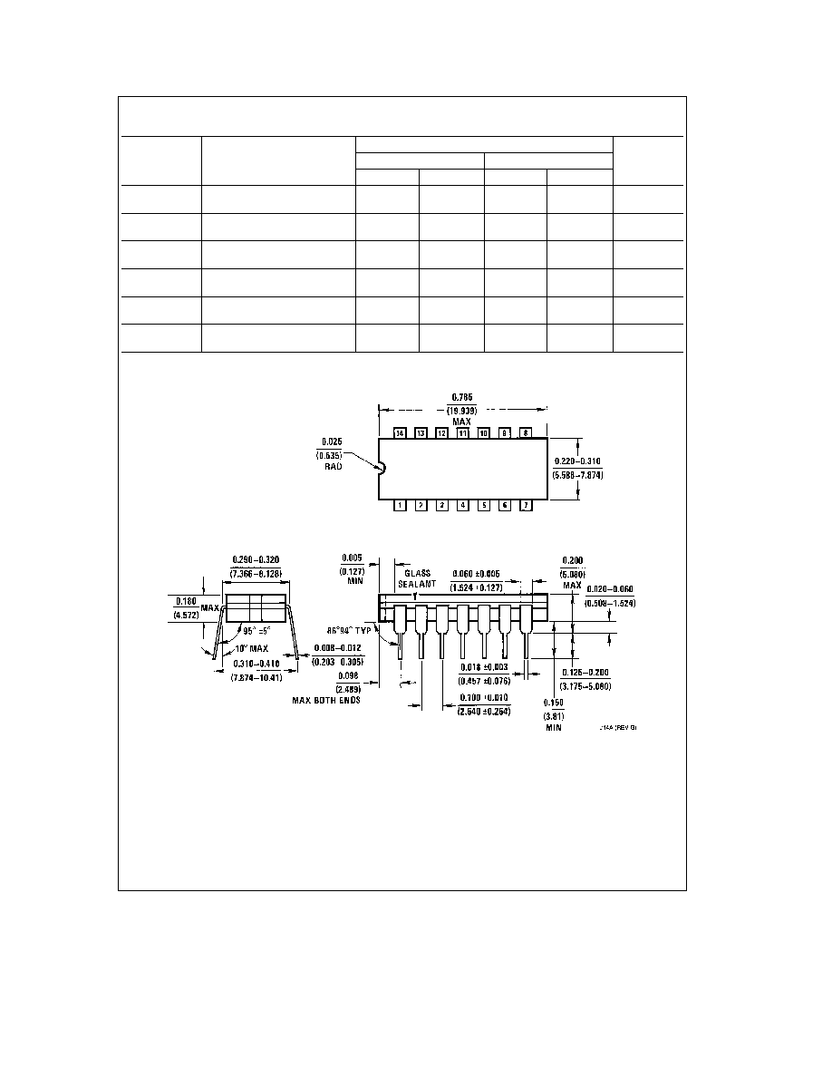
Physical Dimensions
inches (millimeters)
14-Lead Ceramic Dual-In-Line Package (J)
Order Number 54125DMQB or DM54125J
NS Package Number J14A
3

54125DM54125DM74125
Quad
TRI-STATE
Buffers
Physical Dimensions
inches (millimeters) (Continued)
14-Lead Molded Dual-In-Line Package (N)
Order Number DM74125N
NS Package Number N14A
14-Lead Ceramic Flat Package (W)
Order Number 54125FMQB or DM54125W
NS Package Number W14B
LIFE SUPPORT POLICY
NATIONAL'S PRODUCTS ARE NOT AUTHORIZED FOR USE AS CRITICAL COMPONENTS IN LIFE SUPPORT
DEVICES OR SYSTEMS WITHOUT THE EXPRESS WRITTEN APPROVAL OF THE PRESIDENT OF NATIONAL
SEMICONDUCTOR CORPORATION As used herein
1 Life support devices or systems are devices or
2 A critical component is any component of a life
systems which (a) are intended for surgical implant
support device or system whose failure to perform can
into the body or (b) support or sustain life and whose
be reasonably expected to cause the failure of the life
failure to perform when properly used in accordance
support device or system or to affect its safety or
with instructions for use provided in the labeling can
effectiveness
be reasonably expected to result in a significant injury
to the user
National Semiconductor
National Semiconductor
National Semiconductor
National Semiconductor
Corporation
Europe
Hong Kong Ltd
Japan Ltd
1111 West Bardin Road
Fax (a49) 0-180-530 85 86
13th Floor Straight Block
Tel 81-043-299-2309
Arlington TX 76017
Email cnjwge tevm2 nsc com
Ocean Centre 5 Canton Rd
Fax 81-043-299-2408
Tel 1(800) 272-9959
Deutsch Tel (a49) 0-180-530 85 85
Tsimshatsui Kowloon
Fax 1(800) 737-7018
English
Tel (a49) 0-180-532 78 32
Hong Kong
Fran ais Tel (a49) 0-180-532 93 58
Tel (852) 2737-1600
Italiano
Tel (a49) 0-180-534 16 80
Fax (852) 2736-9960
National does not assume any responsibility for use of any circuitry described no circuit patent licenses are implied and National reserves the right at any time without notice to change said circuitry and specifications