
TL F 9478
54F74F138
1-of-8
DecoderDemultiplexer
November 1994
54F 74F138
1-of-8 Decoder Demultiplexer
General Description
The 'F138 is a high-speed 1-of-8 decoder demultiplexer
This device is ideally suited for high-speed bipolar memory
chip select address decoding The multiple input enables
allow parallel expansion to a 1-of-24 decoder using just
three 'F138 devices or a 1-of-32 decoder using four 'F138
devices and one inverter
Features
Y
Demultiplexing capability
Y
Multiple input enable for easy expansion
Y
Active LOW mutually exclusive outputs
Y
Guaranteed 4000V minimum ESD protection
Commercial
Military
Package
Package Description
Number
74F138PC
N16E
16-Lead (0 300 Wide) Molded Dual-In-Line
54F138DM (Note 2)
J16A
16-Lead Ceramic Dual-In-Line
74F138SC (Note 1)
M16A
16-Lead (0 150 Wide) Molded Small Outline JEDEC
74F138SJ (Note 1)
M16D
16-Lead (0 300 Wide) Molded Small Outline EIAJ
54F138FM (Note 2)
W16A
16-Lead Cerpack
54F138LM (Note 2)
E20A
20-Lead Ceramic Leadless Chip Carrier Type C
Note 1
Devices also available in 13
reel Use suffix
e
SCX and SJX
Note 2
Military grade device with environmental and burn-in processing Use suffix
e
DMQB FMQB and LMQB
Logic Symbols
TL F 9478 � 3
IEEE IEC
TL F 9478 � 6
Connection Diagrams
Pin Assignment for DIP
SOIC and Flatpak
TL F 9478 � 1
Pin Assignment
for LCC
TL F 9478 � 2
TRI-STATE
is a registered trademark of National Semiconductor Corporation
C1995 National Semiconductor Corporation
RRD-B30M75 Printed in U S A

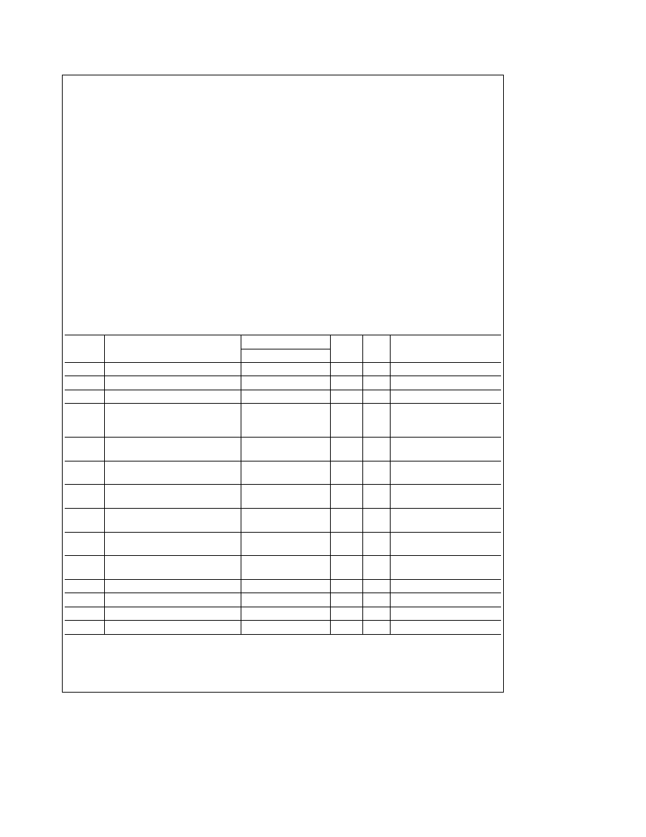
Unit Loading Fan Out
54F 74F
Pin Names
Description
U L
Input I
IH
I
IL
HIGH LOW
Output I
OH
I
OL
A
0
� A
2
Address Inputs
1 0 1 0
20 mA
b
0 6 mA
E
1
E
2
Enable Inputs (Active LOW)
1 0 1 0
20 mA
b
0 6 mA
E
3
Enable Input (Active HIGH)
1 0 1 0
20 mA
b
0 6 mA
O
0
� O
7
Outputs (Active LOW)
50 33 3
b
1 mA 20 mA
Functional Description
The 'F138 high-speed 1-of-8 decoder demultiplexer ac-
cepts three binary weighted inputs (A
0
A
1
A
2
) and when
enabled provides eight mutually exclusive active LOW out-
puts (O
0
� O
7
) The 'F138 features three Enable inputs two
active LOW (E
1
E
2
) and one active HIGH (E
3
) All outputs
will be HIGH unless E
1
and E
2
are LOW and E
3
is HIGH
This multiple enable function allows easy parallel expansion
of the device to a 1-of-32 (5 lines to 32 lines) decoder with
just four 'F138 devices and one inverter (See
Figure 1 ) The
'F138 can be used as an 8-output demultiplexer by using
one of the active LOW Enable inputs as the data input and
the other Enable inputs as strobes The Enable inputs which
are not used must be permanently tied to their appropriate
active HIGH or active LOW state
Truth Table
Inputs
Outputs
E
1
E
2
E
3
A
0
A
1
A
2
O
0
O
1
O
2
O
3
O
4
O
5
O
6
O
7
H
X
X
X
X
X
H
H
H
H
H
H
H
H
X
H
X
X
X
X
H
H
H
H
H
H
H
H
X
X
L
X
X
X
H
H
H
H
H
H
H
H
L
L
H
L
L
L
L
H
H
H
H
H
H
H
L
L
H
H
L
L
H
L
H
H
H
H
H
H
L
L
H
L
H
L
H
H
L
H
H
H
H
H
L
L
H
H
H
L
H
H
H
L
H
H
H
H
L
L
H
L
L
H
H
H
H
H
L
H
H
H
L
L
H
H
L
H
H
H
H
H
H
L
H
H
L
L
H
L
H
H
H
H
H
H
H
H
L
H
L
L
H
H
H
H
H
H
H
H
H
H
H
L
H
e
HIGH Voltage Level
L
e
LOW Voltage Level
X
e
Immaterial
2

Logic Diagram
TL F 9478 � 4
Please note that this diagram is provided only for the understanding of logic operations and should not be used to estimate propagation delays
3
Absolute Maximum Ratings
(Note 1)
If Military Aerospace specified devices are required
please contact the National Semiconductor Sales
Office Distributors for availability and specifications
Storage Temperature
b
65 C to
a
150 C
Ambient Temperature under Bias
b
55 C to
a
125 C
Junction Temperature under Bias
b
55 C to
a
175 C
Plastic
b
55 C to
a
150 C
V
CC
Pin Potential to
Ground Pin
b
0 5V to
a
7 0V
Input Voltage (Note 2)
b
0 5V to
a
7 0V
Input Current (Note 2)
b
30 mA to
a
5 0 mA
Voltage Applied to Output
in HIGH State (with V
CC
e
0V)
Standard Output
b
0 5V to V
CC
TRI-STATE Output
b
0 5V to
a
5 5V
Current Applied to Output
in LOW State (Max)
twice the rated I
OL
(mA)
ESD Last Passing Voltage (Min)
4000V
Note 1
Absolute maximum ratings are values beyond which the device may
be damaged or have its useful life impaired Functional operation under
these conditions is not implied
Note 2
Either voltage limit or current limit is sufficient to protect inputs
Recommended Operating
Conditions
Free Air Ambient Temperature
Military
b
55 C to
a
125 C
Commercial
0 C to
a
70 C
Supply Voltage
Military
a
4 5V to
a
5 5V
Commercial
a
4 5V to
a
5 5V
DC Electrical Characteristics
Symbol
Parameter
54F 74F
Units
V
CC
Conditions
Min
Typ
Max
V
IH
Input HIGH Voltage
2 0
V
Recognized as a HIGH Signal
V
IL
Input LOW Voltage
0 8
V
Recognized as a LOW Signal
V
CD
Input Clamp Diode Voltage
b
1 2
V
Min
I
IN
e b
18 mA
V
OH
Output HIGH
54F 10% V
CC
2 5
I
OH
e b
1 mA
Voltage
74F 10% V
CC
2 5
V
Min
I
OH
e b
1 mA
74F 5% V
CC
2 7
I
OH
e b
1 mA
V
OL
Output LOW
54F 10% V
CC
0 5
V
Min
I
OL
e
20 mA
Voltage
74F 10% V
CC
0 5
I
OL
e
20 mA
I
IH
Input HIGH
54F
20 0
m
A
Max
V
IN
e
2 7V
Current
74F
5 0
I
BVI
Input HIGH Current
54F
100
m
A
Max
V
IN
e
7 0V
Breakdown Test
74F
7 0
I
CEX
Output HIGH
54F
250
m
A
Max
V
OUT
e
V
CC
Leakage Current
74F
50
V
ID
Input Leakage
74F
4 75
V
0 0
I
ID
e
1 9 mA
Test
All Other Pins Grounded
I
OD
Output Leakage
74F
3 75
m
A
0 0
V
IOD
e
150 mV
Circuit Current
All Other Pins Grounded
I
IL
Input LOW Current
b
0 6
mA
Max
V
IN
e
0 5V
I
OS
Output Short-Circuit Current
b
60
b
150
mA
Max
V
OUT
e
0V
I
CCH
Power Supply Current
13
20
mA
Max
V
O
e
HIGH
I
CCL
Power Supply Current
13
20
mA
Max
V
O
e
LOW
4

AC Electrical Characteristics
74F
54F
74F
T
A
e a
25 C
T
A
V
CC
e
Mil
T
A
V
CC
e
Com
Fig
Symbol
Parameter
V
CC
e a
5 0V
C
L
e
50 pF
C
L
e
50 pF
Units
No
C
L
e
50 pF
Min
Typ
Max
Min
Max
Min
Max
t
PLH
Propagation Delay
3 5
5 6
7 5
3 0
12 0
3 5
8 5
ns
F
� 3
t
PHL
A
n
to O
n
4 0
6 1
8 0
4 0
9 5
4 0
9 0
t
PLH
Propagation Delay
3 5
5 4
7 0
3 0
11 0
3 5
8 0
ns
F
� 4
t
PHL
E
1
or E
2
to O
n
3 0
5 3
7 0
3 0
8 0
3 0
7 5
t
PLH
Propagation Delay
4 0
6 2
8 0
3 5
12 5
4 0
9 0
ns
F
� 4
t
PHL
E
3
to O
n
3 5
5 6
7 5
3 5
8 5
3 5
8 5
TL F 9478 � 5
FIGURE 1 Expansion to 1-of-32 Decoding
Ordering Information
The device number is used to form part of a simplified purchasing code where the package type and temperature range are
defined as follows
74F
138
S
C
X
Temperature Range Family
Special Variations
74F
e
Commercial
QB
e
Military grade device with
54F
e
Military
environmental and burn-in
processing
Device Type
X
e
Devices shipped in 13 reel
Package Code
Temperature Range
P
e
Plastic DIP
C
e
Commercial (0 C to
a
70 C)
D
e
Ceramic DIP
M
e
Military (
b
55 C to
a
125 C)
F
e
Flatpak
L
e
Leadless Chip Carrier (LCC)
S
e
Small Outline SOIC JEDEC
SJ
e
Small Outline SOIC EIAJ
5