 | –≠–ª–µ–∫—Ç—Ä–æ–Ω–Ω—ã–π –∫–æ–º–ø–æ–Ω–µ–Ω—Ç: 54165DMQB | –°–∫–∞—á–∞—Ç—å:  PDF PDF  ZIP ZIP |

TL F 9782
54165DM74165
8-Bit
Parallel-to-Serial
Converter
August 1989
54165 DM74165
8-Bit Parallel-to-Serial Converter
General Description
The '165 is an 8-bit parallel load or serial-in register with
complementary outputs available from the last stage Paral-
lel inputting occurs asynchronously when the Parallel Load
(PL) input is LOW With PL HIGH serial shifting occurs on
the rising edge of the clock new data enters via the Serial
Data (D
S
) input The 2-input OR clock can be used to com-
bine two independent clock sources or one input can act as
an active LOW clock enable
Connection Diagram
Dual-In-Line-Package
TL F 9782 ≠ 1
Order Number 54165DMQB 54165FMQB or DM74165N
See NS Package Number J16A N16E or W16A
Logic Symbol
TL F 9782 ≠ 2
V
CC
e
Pin 16
GND
e
Pin 8
Pin Names
Description
CP1 CP2
Clock Pulse Inputs (Active Rising Edge)
D
S
Serial Data Input
PL
Asynchronous Parallel Load Input
(Active LOW)
P0 ≠ P7
Parallel Data Inputs
Q7
Serial Output from Last Stage
Q7
Complementary Output
C1995 National Semiconductor Corporation
RRD-B30M115 Printed in U S A

Absolute Maximum Ratings
(Note)
If Military Aerospace specified devices are required
please contact the National Semiconductor Sales
Office Distributors for availability and specifications
Supply Voltage
7V
Input Voltage
5 5V
Operating Free Air Temperature Range
54
b
55 C to
a
125 C
DM74
0 C to
a
70 C
Storage Temperature Range
b
65 C to
a
150 C
Note
The ``Absolute Maximum Ratings'' are those values
beyond which the safety of the device cannot be guaran-
teed The device should not be operated at these limits The
parametric values defined in the ``Electrical Characteristics''
table are not guaranteed at the absolute maximum ratings
The ``Recommended Operating Conditions'' table will define
the conditions for actual device operation
Recommended Operating Conditions
Symbol
Parameter
54165
DM74165
Units
Min
Nom
Max
Min
Nom
Max
V
CC
Supply Voltage
4 5
5
5 5
4 75
5
5 25
V
V
IH
High Level Input Voltage
2
2
V
V
IL
Low Level Input Voltage
0 8
0 8
V
I
OH
High Level Output Current
b
0 8
b
0 8
mA
I
OL
Low Level Output Current
16
16
mA
T
A
Free Air Operating Temperature
b
55
125
0
70
C
t
s
(H)
Setup Time HIGH or LOW
10
10
ns
t
s
(L)
P
n
to PL
10
10
t
h
(H)
Hold Time HIGH or LOW
10
0
ns
t
h
(L)
P
n
to PL
10
0
t
s
(H)
Setup Time HIGH or LOW
20
20
ns
t
s
(L)
D
S
to CP
n
20
20
t
h
(H)
Hold Time HIGH or LOW
0
0
ns
t
h
(L)
D
S
to CP
n
0
0
t
s
(H)
Setup Time HIGH
30
30
ns
CP1 to CP2 or CP2 to CP1
t
w
(H)
CP
n
Pulse Width HIGH
25
25
ns
t
w
(L)
PL Pulse Width LOW
15
15
ns
t
rec
Recovery Time PL to CP
n
45
45
ns
Electrical Characteristics
Over recommended operating free air temperature range (unless otherwise noted)
Symbol
Parameter
Conditions
Min
Typ
Max
Units
(Note 1)
V
I
Input Clamp Voltage
V
CC
e
Min I
I
e b
12 mA
b
1 5
V
V
OH
High Level Output Voltage
V
CC
e
Min I
OH
e
Max V
IL
e
Max
2 4
3 4
V
V
OL
Low Level Output Voltage
V
CC
e
Min V
IH
e
Min
0 2
0 4
V
I
I
Input Current
Max
V
CC
e
Max V
I
e
5 5V
1
mA
Input Voltage
I
IH
High Level Input Current
V
CC
e
Max V
I
e
2 4V
PL
80
m
A
Inputs
40
I
IL
Low Level Input Current
V
CC
e
Max V
I
e
0 4V
PL
b
3 2
mA
Inputs
b
1 6
I
OS
Short Circuit
V
CC
e
Max
54
b
20
b
55
mA
Output Current
(Note 2)
DM74
b
18
b
55
I
CC
Supply Current
V
CC
e
Max PL
e
63
mA
P
n
e
K CP
1
CP
2
e
4 5V
2

Switching Characteristics
V
CC
e a
5 0V T
A
e a
25 C (See Section 1 for waveforms and load configurations)
C
L
e
15 pF
Symbol
Parameter
R
L
e
400X
Units
Min
Max
f
max
Maximum Clock Frequency
20
MHz
t
PLH
Propagation Delay
31
ns
t
PHL
PL to Q7 or Q7
40
t
PLH
Propagation Delay
24
ns
t
PHL
CP1 to Q7 or Q7
31
t
PLH
Propagation Delay
17
ns
t
PHL
P7 to Q7
36
t
PLH
Propagation Delay
27
ns
t
PHL
P7 to Q7
27
Note 1
All typicals are at V
CC
e
5V T
A
e
25 C
Note 2
Not more than one output should be shorted at a time
Functional Description
The '165 contains eight clocked master slave RS flip-flops
connected as a shift register with auxiliary gating to provide
overriding asynchronous parallel entry Parallel data enters
when the PL signal is LOW The parallel data can change
while PL is LOW provided that the recommended setup and
hold times are observed
For clocked operation PL must be HIGH The two clock
inputs perform identically one can be used as a clock inhibit
by applying a HIGH signal To avoid double clocking how-
ever the inhibit signal should only go HIGH while the clock
is HIGH Otherwise the rising inhibit signal will cause the
same response as a rising clock edge The flip-flops are
edge-triggered for serial operations The serial input data
can change at any time provided only that the recommend-
ed setup and hold times are observed with respect to the
rising edge of the clock
Truth Table
PL
CP
Contents
Response
1
2
Q0
Q1
Q2
Q3
Q4
Q5
Q6
Q7
L
X
X
P0
P1
P2
P3
P4
P5
P6
P7
Parallel Entry
H
L
L
D
S
Q0
Q1
Q2
Q3
Q4
Q5
Q6
Right Shift
H
H
L
Q0
Q1
Q2
Q3
Q4
Q5
Q6
Q7
No Change
H
L
L
D
S
Q0
Q1
Q2
Q3
Q4
Q5
Q6
Right Shift
H
L
H
Q0
Q1
Q2
Q3
Q4
Q5
Q6
Q7
No Change
H
e
HIGH Voltage Level
L
e
LOW Voltage Level
X
e
Immaterial
L
e
Positive Rising Edge
Logic Diagram
TL F 9782 ≠ 3
3

4
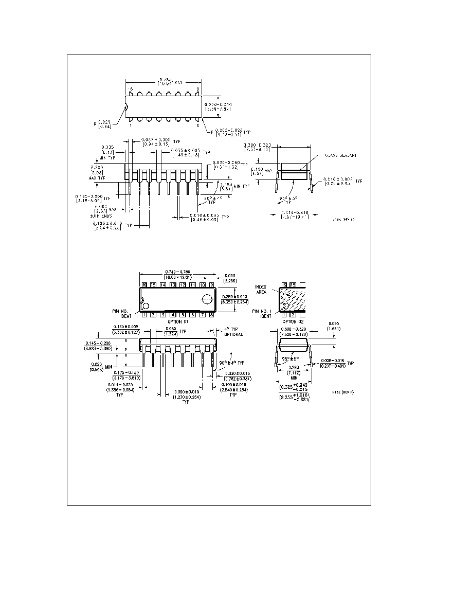
Physical Dimensions
inches (millimeters)
16-Lead Ceramic Dual-In-Line Package (J)
Order Number 54165DMQB
NS Package Number J16A
16-Lead Molded Dual-In-Line Package (N)
Order Number DM74165N
NS Package Number N16E
5