 | –≠–ª–µ–∫—Ç—Ä–æ–Ω–Ω—ã–π –∫–æ–º–ø–æ–Ω–µ–Ω—Ç: 5485 | –°–∫–∞—á–∞—Ç—å:  PDF PDF  ZIP ZIP |
TL F 6530
5485DM5485DM7485
4-Bit
Magnitude
Comparators
June 1989
5485 DM5485 DM7485
4-Bit Magnitude Comparators
General Description
These 4-bit magnitude comparators perform comparison of
straight binary or BCD codes Three fully-decoded decisions
about two 4-bit words (A B) are made and are externally
available at three outputs These devices are fully expand-
able to any number of bits without external gates Words of
greater length may be compared by connecting compara-
tors in cascade The A
l
B A
k
B and A
e
B outputs of a
stage handling less-significant bits are connected to the cor-
responding inputs of the next stage handling more-signifi-
cant bits The stage handling the least-significant bits must
have a high-level voltage applied to the A
e
B input The
cascading paths are implemented with only a two-gate-level
delay to reduce overall comparison times for long words
Features
Y
Typical power dissipation 275 mW
Y
Typical delay (4-bit words) 23 ns
Y
Alternate Military Aerospace device (5485) is available
Contact a National Semiconductor Sales Office Distrib-
utor for specifications
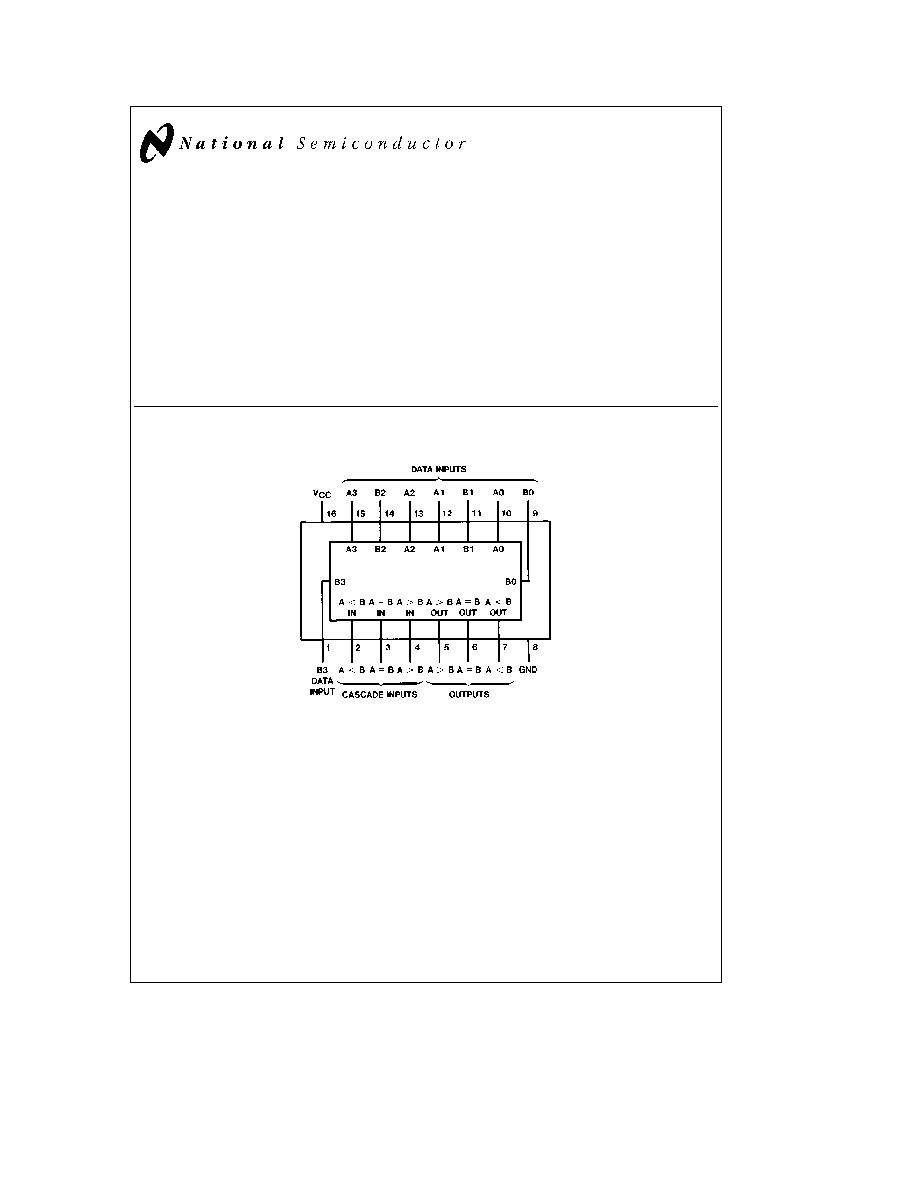
Connection Diagram
Dual-In-Line Package
TL F 6530 ≠ 1
Order Number 5485DMQB 5485FMQB DM5485J DM5485W or DM7485N
See NS Package Number J16A N16E or W16A
C1995 National Semiconductor Corporation
RRD-B30M105 Printed in U S A

Absolute Maximum Ratings
(Note)
If Military Aerospace specified devices are required
please contact the National Semiconductor Sales
Office Distributors for availability and specifications
Supply Voltage
7V
Input Voltage
5 5V
Operating Free Air Temperature Range
DM54 and 54
b
55 C to
a
125 C
DM74
0 C to
a
70 C
Storage Temperature Range
b
65 C to
a
150 C
Note
The ``Absolute Maximum Ratings'' are those values
beyond which the safety of the device cannot be guaran-
teed The device should not be operated at these limits The
parametric values defined in the ``Electrical Characteristics''
table are not guaranteed at the absolute maximum ratings
The ``Recommended Operating Conditions'' table will define
the conditions for actual device operation
Recommended Operating Conditions
Symbol
Parameter
DM5485
DM7485
Units
Min
Nom
Max
Min
Nom
Max
V
CC
Supply Voltage
4 5
5
5 5
4 75
5
5 25
V
V
IH
High Level Input Voltage
2
2
V
V
IL
Low Level Input Voltage
0 8
0 8
V
I
OH
High Level Output Current
b
0 8
b
0 8
mA
I
OL
Low Level Output Current
16
16
mA
T
A
Free Air Operating Temperature
b
55
125
0
70
C
Electrical Characteristics
over recommended operating free air temperature range (unless otherwise noted)
Symbol
Parameter
Conditions
Min
Typ
Max
Units
(Note 1)
V
I
Input Clamp Voltage
V
CC
e
Min I
I
e b
12 mA
b
1 5
V
V
OH
High Level Output
V
CC
e
Min I
OH
e
Max
2 4
V
Voltage
V
IL
e
Max V
IH
e
Min
V
OL
Low Level Output
V
CC
e
Min I
OL
e
Max
0 4
V
Voltage
V
IH
e
Min V
IL
e
Max
I
I
Input Current
Max
V
CC
e
Max V
I
e
5 5V
1
mA
Input Voltage
I
IH
High Level Input
V
CC
e
Max
A
k
B
40
Current
V
I
e
2 4V
A
l
B
40
m
A
Others
120
I
IL
Low Level Input
V
CC
e
Max
A
k
B
b
1 6
Current
V
I
e
0 4V
A
l
B
b
1 6
mA
Others
b
4 8
I
OS
Short Circuit
V
CC
e
Max
DM54
b
20
b
55
mA
Output Current
(Note 2)
DM74
b
18
b
55
I
CC
Supply Current
V
CC
e
Max
55
88
mA
(Note 3)
Note 1
All typicals are at V
CC
e
5V T
A
e
25 C
Note 2
Not more than one output should be shorted at a time
Note 3
I
CC
is measured with all outputs open A
e
B input grounded and all other inputs at 4 5V
2

Switching Characteristics
at V
CC
e
5V and T
A
e
25 C (See Section 1 for Test Waveforms and Output Load)
From
To
Number of
R
L
e
400X
Symbol
Parameter
Input
Output
Gate Levels
C
L
e
15 pF
Units
Min
Max
t
PLH
Propagation Delay Time
Any A or B
A
k
B
3
26
Low-to-High Level Output
Data Input
A
l
B
ns
A
e
B
4
35
t
PHL
Propagation Delay Time
Any A or B
A
k
B
3
30
High-to-Low Level Output
Data Input
A
l
B
ns
A
e
B
4
30
t
PLH
Propagation Delay Time
A
k
B
A
l
B
1
11
ns
Low-to-High Level Output
or A
e
B
t
PHL
Propagation Delay Time
A
k
B
A
l
B
1
17
ns
High-to-Low Level Output
or A
e
B
t
PLH
Propagation Delay Time
A
e
B
A
e
B
2
20
ns
Low-to-High Level Output
t
PHL
Propagation Delay Time
A
e
B
A
e
B
2
17
ns
High-to-Low Level Output
t
PLH
Propagation Delay Time
A
l
B
A
k
B
1
11
ns
Low-to-High Level Output
or A
e
B
t
PHL
Propagation Delay Time
A
l
B
A
k
B
1
17
ns
High-to-Low Level Output
or A
e
B
Function Table
Comparing
Cascading
Outputs
Inputs
Inputs
A3 B3
A2 B2
A1 B1
A0 B0
A
l
B
A
k
B
A
e
B
A
l
B
A
k
B
A
e
B
A3
l
B3
X
X
X
X
X
X
H
L
L
A3
k
B3
X
X
X
X
X
X
L
H
L
A3
e
B3
A2
l
B2
X
X
X
X
X
H
L
L
A3
e
B3
A2
k
B2
X
X
X
X
X
L
H
L
A3
e
B3
A2
e
B2
A1
l
B1
X
X
X
X
H
L
L
A3
e
B3
A2
e
B2
A1
k
B1
X
X
X
X
L
H
L
A3
e
B3
A2
e
B2
A1
e
B1
A0
l
B0
X
X
X
H
L
L
A3
e
B3
A2
e
B2
A1
e
B1
A0
k
B0
X
X
X
L
H
L
A3
e
B3
A2
e
B2
A1
e
B1
A0
e
B0
H
L
L
H
L
L
A3
e
B3
A2
e
B2
A1
e
B1
A0
e
B0
L
H
L
L
H
L
A3
e
B3
A2
e
B2
A1
e
B1
A0
e
B0
L
L
H
L
L
H
A3
e
B3
A2
e
B2
A1
e
B1
A0
e
B0
X
X
H
L
L
H
A3
e
B3
A2
e
B2
A1
e
B1
A0
e
B0
H
H
L
L
L
L
A3
e
B3
A2
e
B2
A1
e
B1
A0
e
B0
L
L
L
H
H
L
H
e
High Level L
e
Low Level X
e
Don't Care
3

Logic Diagram
TL F 6530 ≠ 2
4

Physical Dimensions
inches (millimeters)
16-Lead Ceramic Dual-In-Line Package (J)
Order Number 5485DMQB or DM5485J
NS Package Number J16A
16-Lead Molded Dual-In-Line Package (N)
Order Number DM7485N
NS Package Number N16E
5