 | –≠–ª–µ–∫—Ç—Ä–æ–Ω–Ω—ã–π –∫–æ–º–ø–æ–Ω–µ–Ω—Ç: 54ABT245C | –°–∫–∞—á–∞—Ç—å:  PDF PDF  ZIP ZIP |
54ABT245
Octal Bidirectional Transceiver with TRI-STATE
Æ
Outputs
General Description
The 'ABT245 contains eight non-inverting bidirectional buff-
ers with TRI-STATE outputs and is intended for bus-oriented
applications. Current sinking capability is 48 mA on both the
A and B ports. The Transmit/Receive (T/R) input determines
the direction of data flow through the bidirectional trans-
ceiver. Transmit (active HIGH) enables data from A ports to B
ports; Receive (active LOW) enables data from B ports to A
ports. The Output Enable input, when HIGH, disables both A
and B ports by placing them in a High Z condition.
Features
n
Bidirectional non-inverting buffers
n
A and B output sink capability of 48 mA, source
capability of 24 mA
n
Guaranteed output skew
n
Guaranteed multiple output switching specifications
n
Output switching specified for both 50 pF and 250 pF
loads
n
Guaranteed simultaneous switching, noise level and
dynamic threshold performance
n
Guaranteed latchup protection
n
High impedance glitch-free bus loading during entire
power up and power down cycle
n
Non-destructive hot insertion capability
n
Disable time is less than enable time to avoid bus
contention
n
Standard Microcircuit Drawing (SMD) 5962-9214801
Ordering Code:
Military
Package
Package Description
Number
54ABT245J-QML
J20A
20-Lead Ceramic Dual-In-Line
54ABT245W-QML
W20A
20-Lead Cerpak
54ABT245E-QML
E20A
20-Lead Ceramic Leadless Chip Carrier, Type C
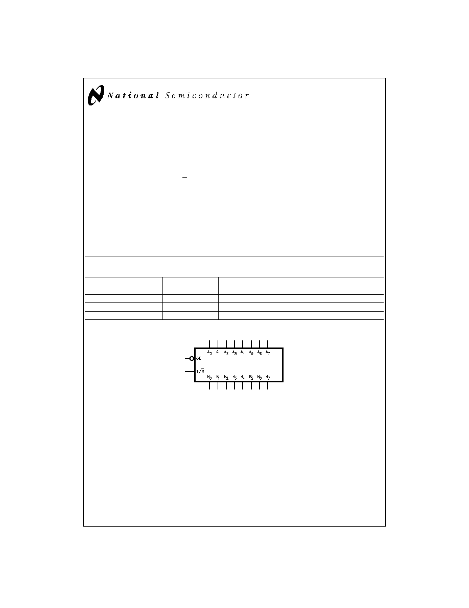
Logic Symbol
TRI-STATE
Æ
is a registered trademark of National Semiconductor Corporation.
DS100204-1
July 1998
54ABT245
Octal
Bidirectional
T
ransceiver
with
TRI-ST
A
T
E
Outputs
© 1998 National Semiconductor Corporation
DS100204
www.national.com

Connection Diagrams
Pin Descriptions
Pin Names
Description
OE
Output Enable Input (Active LOW)
T/R
Transmit/Receive Input
A
0
≠A
7
Side A Inputs or TRI-STATE Outputs
B
0
≠B
7
Side B Inputs or TRI-STATE Outputs
Truth Table
Inputs
Output
OE
T/R
L
L
Bus B Data to Bus A
L
H
Bus A Data to Bus B
H
X
High Z State
H = HIGH Voltage Level
L = LOW Voltage Level
X = Immaterial
Logic Diagram
Pin Assignment for DIP
and Flatpak.
DS100204-5
Pin Assignment for LCC
DS100204-3
DS100204-4
www.national.com
2
Absolute Maximum Ratings
(Note 1)
If Military/Aerospace specified devices are required,
please contact the National Semiconductor Sales Office/
Distributors for availability and specifications.
Storage Temperature
-65∞C to +150∞C
Ambient Temperature under Bias
-55∞C to +125∞C
Junction Temperature under Bias
Ceramic
-55∞C to +175∞C
V
CC
Pin Potential to
Ground Pin
-0.5V to +7.0V
Input Voltage (Note 2)
-0.5V to +7.0V
Input Current (Note 2)
-30 mA to +5.0 mA
Voltage Applied to Any Output
in the Disabled or
Power-off State
-0.5V to 5.5V
in the HIGH State
-0.5V to V
CC
Current Applied to Output
in LOW State (Max)
twice the rated I
OL
(mA)
DC Latchup Source Current
-500 mA
Over Voltage Latchup (I/O)
10V
Recommended Operating
Conditions
Free Air Ambient Temperature
Military
-55∞C to +125∞C
Supply Voltage
Military
+4.5V to +5.5V
Minimum Input Edge Rate
(
V/
t)
Data Input
50 mV/ns
Enable Input
20 mV/ns
Note 1: Absolute maximum ratings are values beyond which the device may
be damaged or have its useful life impaired. Functional operation under these
conditions is not implied.
Note 2: Either voltage limit or current limit is sufficient to protect inputs.
DC Electrical Characteristics
Symbol
Parameter
ABT245
Units
V
CC
Conditions
Min
Typ
Max
V
IH
Input HIGH Voltage
2.0
V
Recognized HIGH Signal
V
IL
Input LOW Voltage
0.8
V
Recognized LOW Signal
V
CD
Input Clamp Diode Voltage
-1.2
V
Min
I
IN
= -18 mA (OE, T/R)
V
OH
Output HIGH
Voltage
54ABT
2.5
V
Min
I
OH
= -3 mA (A
n
, B
n
)
54ABT
2.0
V
Min
I
OH
= -24 mA (A
n
, B
n
)
V
OL
Output LOW
Voltage
54ABT
0.55
V
Min
I
OL
= 48 mA (A
n
, B
n
)
I
IH
Input HIGH Current
5
µA
Max
V
IN
= 2.7V (OE, T/R) (Note 3)
5
V
IN
= V
CC
(OE, T/R)
I
BVI
Input HIGH Current Breakdown Test
7
µA
Max
V
IN
= 7.0V (OE, T/R)
I
BVIT
Input HIGH Current Breakdown Test
(I/O)
100
µA
Max
V
IN
= 5.5V (A
n
, B
n
)
I
IL
Input LOW Current
-5
µA
Max
V
IN
= 0.5V (OE, T/R) (Note 3)
-5
V
IN
= 0.0V (OE, T/R)
V
ID
Input Leakage Test
4.75
V
0.0
I
ID
= 1.9 µA (OE, T/R)
All Other Pins Grounded
I
IH
+ I
OZH
Output Leakage Current
50
µA
0 - 5.5V
V
OUT
= 2.7V (A
n
, B
n
); OE = 2.0V
I
IL
+ I
OZL
Output Leakage Current
-50
µA
0 - 5.5V
V
OUT
= 0.5V (A
n
, B
n
); OE = 2.0V
I
OS
Output Short-Circuit Current
-100
-275
mA
Max
V
OUT
= 0.0V (A
n
, B
n
)
I
CEX
Output High Leakage Current
50
µA
Max
V
OUT
= V
CC
(A
n
, B
n
)
I
ZZ
Bus Drainage Test
100
µA
0.0
V
OUT
= 5.5V (A
n
, B
n
);
All Others GND
I
CCH
Power Supply Current
50
µA
Max
All Outputs HIGH
I
CCL
Power Supply Current
30
mA
Max
All Outputs LOW
I
CCZ
Power Supply Current
50
µA
Max
OE = V
CC
, T/R = GND or V
CC
;
All Other GND or V
CC
I
CCT
Additional
Outputs Enabled
2.5
mA
V
I
= V
CC
- 2.1V
I
CC
/Input
Outputs TRI-STATE
2.5
mA
Max
OE, T/R V
I
= V
CC
- 2.1V
Outputs TRI-STATE
50
µA
Data Input V
I
= V
CC
- 2.1V
All Others at V
CC
or GND.
3
www.national.com

DC Electrical Characteristics
(Continued)
Symbol
Parameter
ABT245
Units
V
CC
Conditions
Min
Typ
Max
I
CCD
Dynamic I
CC
No Load
0.1
mA/
MHz
Max
Outputs Open
(Note 3)
OE = GND, T/R = GND or V
CC
One Bit Toggling, 50% Duty Cycle
(Note 4)
Note 3: Guaranteed but not tested.
Note 4: For 8 bits toggling, I
CCD
<
0.8 mA/MHz.
DC Electrical Characteristics
Conditions
Symbol
Parameter
Min
Max
Units
V
CC
C
L
= 50 pF,
R
L
= 500
V
OLP
Quiet Output Maximum Dynamic V
OL
1.1
V
5.0
T
A
= 25∞C (Note 5)
V
OLV
Quiet Output Minimum Dynamic V
OL
-0.45
V
5.0
T
A
= 25∞C(Note 5)
Note 5: Max number of outputs defined as (n). n - 1 data inputs are driven 0V to 3V. One output at LOW.
AC Electrical Characteristics
Symbol
Parameter
54ABT
Units
T
A
= -55∞C to +125∞C
V
CC
= 4.5V≠5.5V
C
L
= 50 pF
Min
Max
t
PLH
Propagation Delay
1.0
4.8
ns
t
PHL
Data to Outputs
1.0
4.8
t
PZH
Output Enable
1.0
6.7
ns
t
PZL
Time
2.0
7.5
t
PHZ
Output Disable
1.7
7.4
ns
t
PLZ
Time
1.7
6.5
Capacitance
Symbol
Parameter
Typ
Units
Conditions
T
A
= 25∞C
C
IN
Input Capacitance
5.0
pF
V
CC
= 0V (OE , T/R)
C
I/O
(Note 6)
I/O Capacitance
11.0
pF
V
CC
= 5.0V (A
n
, B
n
)
Note 6: C
I/O
is measured at frequency f = 1 MHz, per MIL-STD-883B, Method 3012.
www.national.com
4
Capacitance
(Continued)
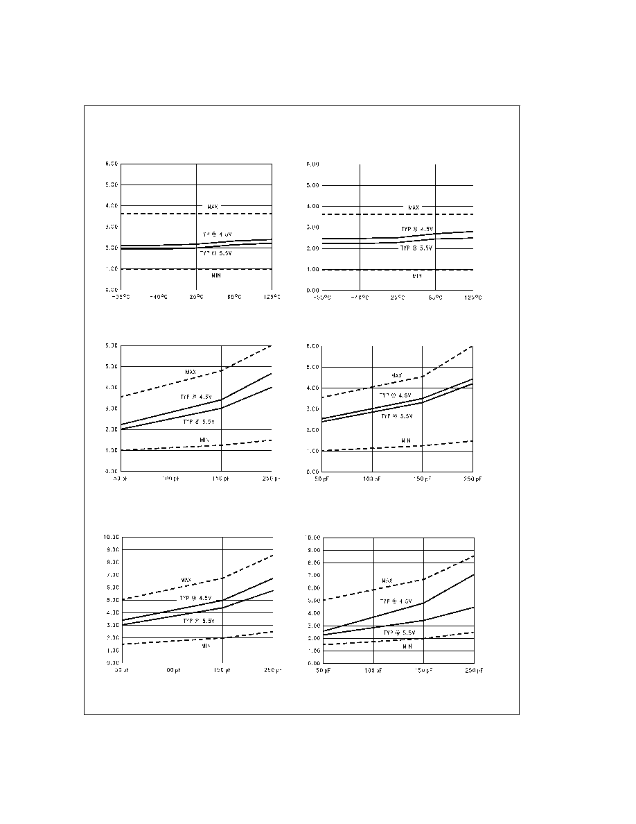
Dashed lines represent design characteristics; for specified guarantees, refer to AC Characteristics Table.
t
PLH
vs Temperature (T
A
)
C
L
= 50 pF, 1 Output Switching
DS100204-14
t
PHL
vs Temperature (T
A
)
C
L
= 50 pF, 1 Output Switching
DS100204-15
t
PLH
vs Load Capacitance
1 Output Switching, T
A
= 25∞C
DS100204-16
t
PHL
vs Load Capacitance
1 Output Switching, T
A
= 25∞C
DS100204-17
t
PLH
vs Load Capacitance
8 Outputs Switching, T
A
= -40∞C to +85∞C
DS100204-18
t
PHL
vs Load Capacitance
8 Outputs Switching, T
A
= 25∞C
DS100204-19
5
www.national.com