
54AC175
∑
54ACT175
Quad D Flip-Flop
General Description
The 'AC/'ACT175 is a high-speed quad D flip-flop. The de-
vice is useful for general flip-flop requirements where clock
and clear inputs are common. The information on the D in-
puts is stored during the LOW-to-HIGH clock transition. Both
true and complemented outputs of each flip-flop are pro-
vided. A Master Reset input resets all flip-flops, independent
of the Clock or D inputs, when LOW.
Features
n
Edge-triggered D-type inputs
n
Buffered positive edge-triggered clock
n
Asynchronous common reset
n
True and complement output
n
Outputs source/sink 24 mA
n
'ACT175 has TTL-compatible inputs
n
Standard Microcircuit Drawing (SMD)
-- 'AC175: 5962-89552
-- 'ACT175: 5962-89693
Logic Symbols
Pin Names
Description
D
0
≠D
3
Data Inputs
CP
Clock Pulse Input
MR
Master Reset Input
Q
0
≠Q
3
True Outputs
Q
0
≠Q
3
Complement Outputs
Connection Diagrams
FACT
Æ
is a registered trademark of Fairchild Semiconductor Corporation.
DS100278-1
IEEE/IEC
DS100278-2
Pin Assignment
for DIP and Flatpak
DS100278-3
Pin Assignment for LCC
DS100278-4
August 1998
54AC175
∑
54ACT175
Quad
D
Flip-Flop
© 1998 National Semiconductor Corporation
DS100278
www.national.com
Functional Description
The 'AC/'ACT175 consists of four edge-triggered D flip-flops
with individual D inputs and Q and Q outputs. The Clock and
Master Reset are common. The four flip-flops will store the
state of their individual D inputs on the LOW-to-HIGH clock
(CP) transition, causing individual Q and Q outputs to follow.
A LOW input on the Master Reset (MR) will force all Q out-
puts LOW and Q outputs HIGH independent of Clock or Data
inputs. The 'AC/'ACT175 is useful for general logic applica-
tions where a common Master Reset and Clock are
acceptable.
Truth Table
Inputs
Outputs
@
t
n
, MR = H
@
t
n+1
D
n
Q
n
Q
n
L
L
H
H
H
L
H = HIGH Voltage Level
L = LOW Voltage Level
t
n
= Bit Time before Clock Pulse
t
n+1
= Bit Time after Clock Pulse
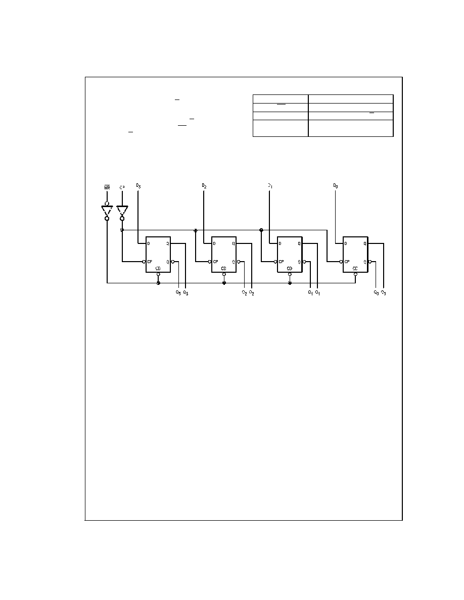
Logic Diagram
DS100278-5
Please note that this diagram is provided only for the understanding of logic operations and should not be used to estimate propagation delays.
www.national.com
2

Absolute Maximum Ratings
(Note 1)
If Military/Aerospace specified devices are required,
please contact the National Semiconductor Sales Office/
Distributors for availability and specifications.
Supply Voltage (V
CC
)
-0.5V to +7.0V
DC Input Diode Current (I
IK
)
V
I
= -0.5V
-20 mA
V
I
= V
CC
+ 0.5V
+20 mA
DC Input Voltage (V
I
)
-0.5V to V
CC
+ 0.5V
DC Output Diode Current (I
OK
)
V
O
= -0.5V
-20 mA
V
O
= V
CC
+ 0.5V
+20 mA
DC Output Voltage (V
O
)
-0.5V to V
CC
+ 0.5V
DC Output Source
or Sink Current (I
O
)
±
50 mA
DC V
CC
or Ground Current
per Output Pin (I
CC
or I
GND
)
±
50 mA
Storage Temperature (T
STG
)
-65∞C to +150∞C
Junction Temperature (T
J
)
CDIP
175∞C
Recommended Operating
Conditions
Supply Voltage (V
CC
)
'AC
2.0V to 6.0V
'ACT
4.5V to 5.5V
Input Voltage (V
I
)
0V to V
CC
Output Voltage (V
O
)
0V to V
CC
Operating Temperature (T
A
)
54AC/ACT
-55∞C to +125∞C
Minimum Input Edge Rate (
V/
t)
'AC Devices
V
IN
from 30% to 70% of V
CC
V
CC
@
3.3V, 4.5V, 5.5V
125 mV/ns
Minimum Input Edge Rate (
V/
t)
'ACT Devices
V
IN
from 0.8V to 2.0V
V
CC
@
4.5V, 5.5V
125 mV/ns
Note 1: Absolute maximum ratings are those values beyond which damage
to the device may occur. The databook specifications should be met, without
exception, to ensure that the system design is reliable over its power supply,
temperature, and output/input loading variables. National does not recom-
mend operation of FACT
Æ
circuits outside databook specifications.
DC Characteristics for 'AC Family Devices
54AC
Symbol
Parameter
V
CC
T
A
= -55∞C to +125∞C
Units
Conditions
(V)
Guaranteed Limits
V
IH
Minimum High Level
3.0
2.1
V
OUT
= 0.1V
Input Voltage
4.5
3.15
V
or V
CC
- 0.1V
5.5
3.85
V
IL
Maximum Low Level
3.0
0.9
V
OUT
= 0.1V
Input Voltage
4.5
1.35
V
or V
CC
- 0.1V
5.5
1.65
V
OH
Minimum High Level
3.0
2.9
I
OUT
= -50 µA
Output Voltage
4.5
4.4
V
5.5
5.4
(Note 2)
V
IN
= V
IL
or V
IH
3.0
2.4
I
OH
= -12 mA
4.5
3.7
V
I
OH
= -24 mA
5.5
4.7
I
OH
= -24 mA
V
OL
Maximum Low Level
3.0
0.1
I
OUT
= 50 µA
Output Voltage
4.5
0.1
V
5.5
0.1
(Note 2)
V
IN
= V
IL
or V
IH
3.0
0.50
I
OL
= 12 mA
4.5
0.50
V
I
OL
= 24 mA
5.5
0.50
I
OL
= 24 mA
I
IN
Maximum Input
5.5
±
1.0
µA
V
I
= V
CC
, GND
Leakage Current
(Note 3)
I
OLD
Minimum Dynamic
5.5
50
mA
V
OLD
= 1.65V Max
I
OHD
Output Current
5.5
-50
mA
V
OHD
= 3.85V Min
3
www.national.com

DC Characteristics for 'AC Family Devices
(Continued)
54AC
Symbol
Parameter
V
CC
T
A
= -55∞C to +125∞C
Units
Conditions
(V)
Guaranteed Limits
I
CC
Maximum Quiescent
5.5
160.0
µA
V
IN
= V
CC
Supply Current
or GND
Note 2: All outputs loaded; thresholds on input associated with output under test.
Note 3: Maximum test duration 2.0 ms, one output loaded at a time.
Note 4: I
IN
and I
CC
@
3.0V are guaranteed to be less than or equal to the respective limit
@
5.5V V
CC
.
I
CC
for 54AC
@
25∞C is identical to 74AC
@
25∞C.
DC Characteristics for 'ACT Family Devices
54ACT
Symbol
Parameter
V
CC
T
A
= -55∞C to +125∞C
Units
Conditions
(V)
Guaranteed Limits
V
IH
Minimum High Level
4.5
2.0
V
V
OUT
= 0.1V
Input Voltage
5.5
2.0
or V
CC
- 0.1V
V
IL
Maximum Low Level
4.5
0.8
V
V
OUT
= 0.1V
Input Voltage
5.5
0.8
or V
CC
- 0.1V
V
OH
Minimum High Level
4.5
4.4
V
I
OUT
= -50 µA
Output Voltage
5.5
5.4
(Note 5)
V
IN
= V
IL
or V
IH
4.5
3.70
V
I
OH
= -24 mA
5.5
4.70
I
OH
= -24 mA
V
OL
Maximum Low Level
4.5
0.1
V
I
OUT
= 50 µA
Output Voltage
5.5
0.1
(Note 5)
V
IN
= V
IL
or V
IH
4.5
0.50
V
I
OL
= 24 mA
5.5
0.50
I
OL
= 24 mA
I
IN
Maximum Input
5.5
±
1.0
µA
V
I
= V
CC
, GND
Leakage Current
I
CCT
Maximum
5.5
1.6
mA
V
I
= V
CC
- 2.1V
I
CC
/Input
(Note 6)
I
OLD
Minimum Dynamic
5.5
50
mA
V
OLD
= 1.65V Max
I
OHD
Output Current
5.5
-50
mA
V
OHD
= 3.85V Min
I
CC
Maximum Quiescent
5.5
160.0
µA
V
IN
= V
CC
Supply Current
or GND
Note 5: All outputs loaded; thresholds on input associated with output under test.
Note 6: Maximum test duration 2.0 ms, one output loaded at a time.
Note 7: I
CC
for 54ACT
@
25∞C is identical to 74ACT
@
25∞C.
www.national.com
4

AC Electrical Characteristics
Symbol
Parameter
54AC
Units
V
CC
T
A
= -55∞C to +125∞C
Fig.
(V)
C
L
= 50 pF
No.
(Note 8)
Min
Max
f
max
Maximum Clock
3.3
95
MHz
Frequency
5.0
95
t
PLH
Propagation Delay
3.3
1.0
14.5
ns
CP to Q
n
or Q
n
5.0
1.5
10.5
t
PHL
Propagation Delay
3.3
1.0
15.0
ns
CP to Q
n
or Q
n
5.0
1.5
11.5
t
PLH
Propagation Delay
3.3
1.0
15.0
ns
MR to Q
n
5.0
1.5
11.0
t
PHL
Propagation Delay
3.3
1.0
13.5
ns
MR to Q
n
5.0
1.5
10.5
Note 8: Voltage Range 3.3 is 3.3V
±
0.3V
Voltage Range 5.0 is 5.0V
±
0.5V
AC Operating Requirements
Symbol
Parameter
54AC
Units
V
CC
T
A
= -55∞C to +125∞C
Fig.
(V)
C
L
= 50 pF
No.
(Note 9)
Guaranteed Minimum
t
s
Setup Time, HIGH or LOW
3.3
5.0
ns
D
n
to CP
5.0
3.5
t
h
Hold Time, HIGH or LOW
3.3
2.0
ns
D
n
to CP
5.0
2.5
t
w
CP Pulse Width
3.3
6.0
ns
HIGH or LOW
5.0
5.0
t
w
MR Pulse Width, LOW
3.3
5.5
ns
5.0
5.0
t
rec
Recovery Time
3.3
1.5
ns
MR to CP
5.0
1.5
Note 9: Voltage Range 3.3 is 3.3V
±
0.3V
Voltage Range 5.0 is 5.0V
±
0.5V
5
www.national.com