 | –≠–ª–µ–∫—Ç—Ä–æ–Ω–Ω—ã–π –∫–æ–º–ø–æ–Ω–µ–Ω—Ç: 54ACT399D | –°–∫–∞—á–∞—Ç—å:  PDF PDF  ZIP ZIP |
54ACT399
Quad 2-Port Register
General Description
The 'AC/ACT399 is the logical equivalent of a quad 2-input
multiplexer feeding into four edge-triggered flip-flops. A com-
mon Select input determines which of the two 4-bit words is
accepted. The selected data enters the flip-flop on the rising
edge of the clock.
Features
n
I
CC
reduced by 50%
n
Select inputs from two data sources
n
Fully positive edge-triggered operation
n
Outputs source/sink 24 mA
n
ACT399 has TTL-compatible inputs
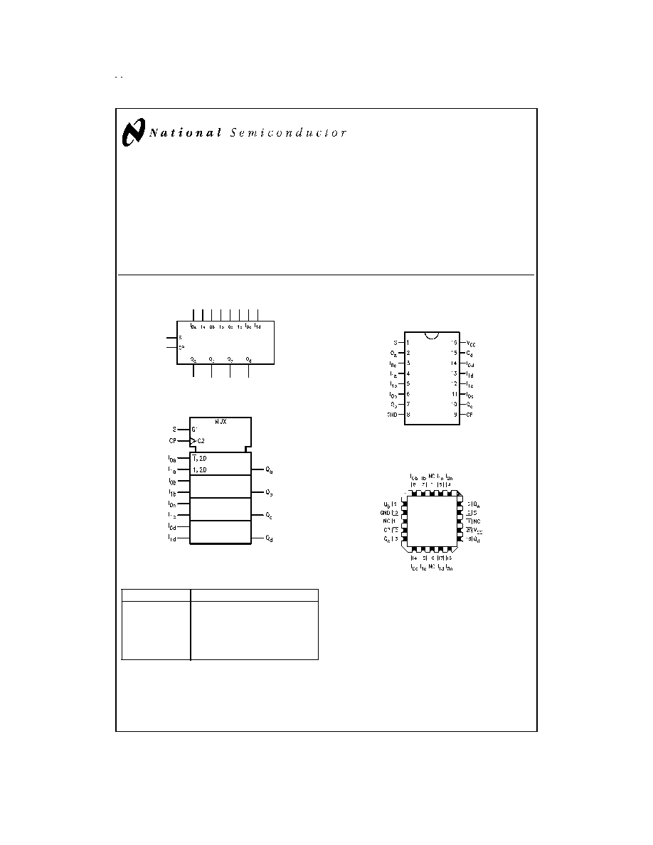
Logic Symbols
Connection Diagrams
Pin Names
Description
S
Common Select Input
CP
Clock Pulse Input
I
0a
≠I
0d
Data Inputs from Source 0
I
1a
≠I
1d
Data Inputs from Source 1
Q
a
≠Q
d
Register True Outputs
TRI-STATE
Æ
is a registered trademark of National Semiconductor Corporation.
FACT
Æ
is a registered trademark of Fairchild Semiconductor Corporation.
DS100356-1
IEEE/IEC
DS100356-5
Pin Assignment
for DIP and Flatpak
DS100356-3
Pin Assignment
for LCC
DS100356-2
August 1998
54ACT399
Quad
2-Port
Register
© 1998 National Semiconductor Corporation
DS100356
www.national.com

Functional Description
The 'AC/ACT399 is a high-speed quad 2-port register. It se-
lects four bits of data from either of two sources (Ports) un-
der control of a common Select input (S). The selected data
is transferred to a 4-bit output register synchronous with the
LOW-to-HIGH transition of the Clock input (CP). The 4-bit
D-type output register is fully edge-triggered. The Data in-
puts (I
0x
, I
1x
) and Select input (S) must be stable only a setup
time prior to and hold time after the LOW-to-HIGH transition
of the Clock input for predictable operation.
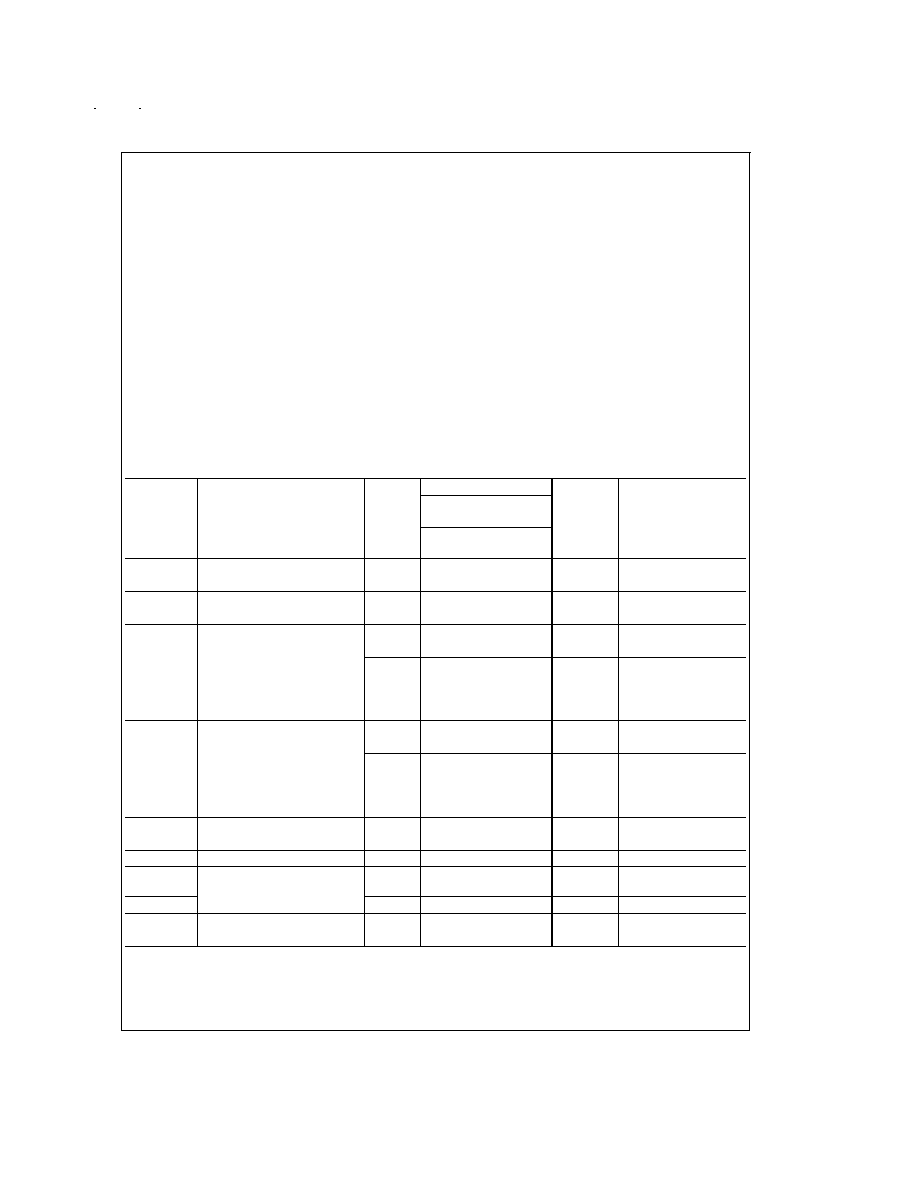
Function Table
Inputs
Outputs
S
I
0
I
1
CP
Q
Q
L
L
X
N
L
H
L
H
X
N
H
L
H
X
L
N
L
H
H
X
H
N
H
L
H = HIGH Voltage Level
L = LOW Voltage Level
X = Immaterial
N
= LOW-to-HIGH Clock Transition
Logic Diagram
DS100356-4
Please note that this diagram is provided only for the understanding of logic operations and should not be used to estimate propagation delays.
www.national.com
2
Absolute Maximum Ratings
(Note 1)
If Military/Aerospace specified devices are required,
please contact the National Semiconductor Sales Office/
Distributors for availability and specifications.
Supply Voltage (V
CC
)
-0.5V to +7.0V
DC Input Diode Current (I
IK
)
V
I
= -0.5V
-20 mA
V
I
= V
CC
+ 0.5V
+20 mA
DC Input Voltage (V
I
)
-0.5V to V
CC
+ 0.5V
DC Output Diode Current (I
OK
)
V
O
= -0.5V
-20 mA
V
O
= V
CC
+ 0.5V
+20 mA
DC Output Voltage (V
O
)
-0.5V to V
CC
+ 0.5V
DC Output Source or
Sink Current (I
O
)
±
50 mA
DC V
CC
or Ground Current
per Output Pin (I
CC
or I
GND
)
±
50 mA
Storage Temperature (T
STG
)
-65∞C to +150∞C
Junction Temperature (T
J
)
CDIP
+175∞C
Recommended Operating
Conditions
Supply Voltage (V
CC
)
'ACT
4.5V to 5.5V
Input Voltage (V
I
)
0V to V
CC
Output Voltage (V
O
)
0V to V
CC
Operating Temperature (T
A
)
54ACT
-55∞C to +125∞C
Minimum Input Edge Rate (
V/
t)
'ACT Devices
V
IN
from 0.8V to 2.0V
V
CC
@
4.5V, 5.5V
125 mV/ns
Note 1: Absolute maximum ratings are those values beyond which damage
to the device may occur. The databook specifications should be met, without
exception, to ensure that the system design is reliable over its power supply,
temperature, and output/input loading variables. National does not recom-
mend operation of FACT
Æ
circuits outside databook specifications.
DC Electrical Characteristics for 'ACT Family Devices
54ACT
Symbol
Parameter
V
CC
T
A
= -55∞C to
+125∞C
Units
Conditions
(V)
Guaranteed
Limits
V
IH
Minimum High Level
4.5
2.0
V
V
OUT
= 0.1V
Input Voltage
5.5
2.0
or V
CC
-0.1V
V
IL
Maximum Low Level
4.5
0.8
V
V
OUT
= 0.1V
Input Voltage
5.5
0.8
or V
CC
- 0.1V
V
OH
Minimum High Level
4.5
4.4
V
I
OUT
= -50 µA
5.5
5.4
(Note 2)
V
IN
= V
IL
or V
IH
4.5
3.70
V
I
OH
= -24 mA
5.5
4.70
I
OH
= -24 mA
V
OL
Maximum Low Level
4.5
0.1
V
I
OUT
= 50 µA
Output Voltage
5.5
0.1
(Note 2)
V
IN
= V
IL
or V
IH
4.5
0.50
V
I
OL
= 24 mA
5.5
0.50
I
OL
= 24 mA
I
IN
Maximum Input
5.5
±
1.0
µA
V
I
= V
CC
, GND
Leakage Current
I
CCT
Maximum I
CC
/Input
5.5
1.6
mA
V
I
= V
CC
-2.1V
I
OLD
Minimum Dynamic
(Note 3)
5.5
50
mA
V
OLD
= 1.65V Max
I
OHD
Output Current
5.5
-50
mA
V
OHD
= 3.85V Min
I
CC
Maximum Quiescent
5.5
80.0
µA
V
IN
= V
CC
Supply Current
or Ground
Note 2: All outputs loaded; thresholds on input associated with output under test.
Note 3: Maximum test duration 2.0 ms, one output loaded at a time.
www.national.com
3

AC Electrical Characteristics
54ACT
V
CC
T
A
, V
CC
= Mil
Fig.
Symbol
Parameter
(V)
C
L
= 50 pF
Units
No.
(Note 4)
Min
Max
f
max
Input Clock Frequency
5.0
90
MHz
t
PLH
Propagation Delay
5.0
1.5
10.0
ns
CP to Q
t
PHL
Propagation Delay
5.0
1.5
10.0
ns
CP to Q
Note 4: Voltage Range 5.0 is 5.0V
±
0.5V
AC Operating Requirements
54ACT
V
CC
T
A
= -55∞C
Units
Fig.
Symbol
Parameter
(V)
to +125∞C
No.
(Note 5)
C
L
= 50 pF
Guaranteed
Minimum
t
s
Setup Time, HIGH or LOW
5.0
3.5
ns
I
n
to CP
t
h
Hold Time, HIGH or LOW
5.0
3.0
ns
I
n
to CP
t
s
Setup Time, HIGH or LOW
5.0
6.0
ns
S to CP
t
h
Hold Time, HIGH or LOW
5.0
2.5
ns
S to CP
t
w
CP Pulse Width,
5.0
5.0
ns
HIGH or LOW
Note 5: Voltage Range 5.0 is 5.0V
±
0.5V
Capacitance
Symbol
Parameter
Typ
Units
Conditions
C
IN
Input Capacitance
4.5
pF
V
CC
= OPEN
C
PD
Power Dissipation Capacitance
30
pF
V
CC
= 5.0V
www.national.com
4

Physical Dimensions
inches (millimeters) unless otherwise noted
20 Terminal Ceramic Leadless Chip Carrier (L)
NS Package Number E20A
16-Lead Ceramic Dual-In-Line Package (D)
NS Package Number J16A
www.national.com
5