 | –≠–ª–µ–∫—Ç—Ä–æ–Ω–Ω—ã–π –∫–æ–º–ø–æ–Ω–µ–Ω—Ç: 54ACT564D | –°–∫–∞—á–∞—Ç—å:  PDF PDF  ZIP ZIP |
54ACT564
Octal D-Type Flip-Flop with TRI-STATE
Æ
Outputs
General Description
The 'ACT564 is a high-speed, low power octal flip-flop with a
buffered common Clock (CP) and a buffered common Out-
put Enable (OE). The information presented to the D inputs
is stored in the flip-flops on the LOW-to-HIGH Clock (CP)
transition.
The 'ACT564 is functionally identical to the 'ACT574, but
with inverted outputs.
Features
n
I
CC
and I
OZ
reduced by 50%
n
Inputs and outputs on opposite sides of package
allowing easy interface with microprocessors
n
Useful as input or output port for microprocessors
n
Functionally identical to 'ACT574 but with inverted
outputs
n
TRI-STATE outputs for bus-oriented applications
n
Outputs source/sink 24 mA
n
'ACT564 has TTL-compatible inputs
n
Standard Microcircuit Drawing (SMD) 5962-89557
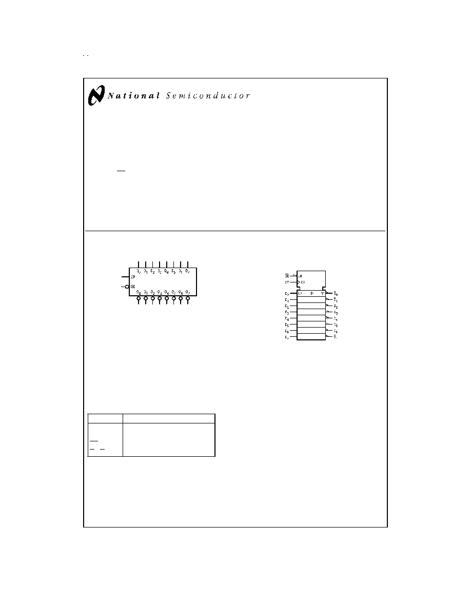
Logic Symbols
Pin Names
Description
D
0
≠D
7
Data Inputs
CP
Clock Pulse Input
OE
TRI-STATE Output Enable Input
O
0
≠O
7
TRI-STATE Outputs
TRI-STATE
Æ
is a registered trademark of National Semiconductor Corporation.
FACT
TM
is a trademark of Fairchild Semiconductor Corporation.
DS100994-1
IEEE/IEC
DS100994-2
September 1998
54ACT564
Octal
D-T
ype
Flip-Flop
with
TRI-ST
A
T
E
Outputs
© 1998 National Semiconductor Corporation
DS100994
www.national.com
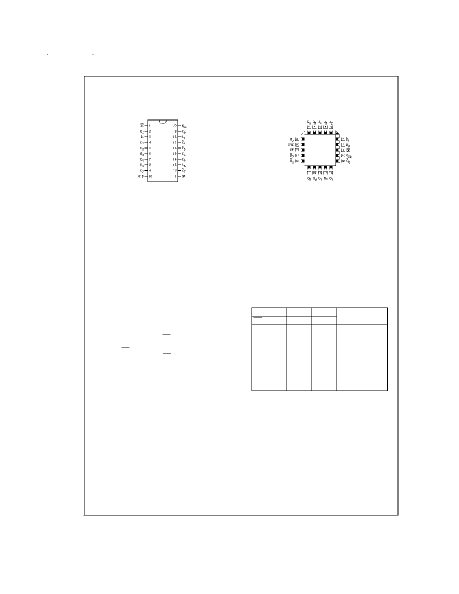
Connection Diagrams
Functional Description
The'ACT564 consists of eight edge-triggered flip-flops with
individual D-type inputs and TRI-STATE complement out-
puts. The buffered clock and buffered Output Enable are
common to all flip-flops. The eight flip-flops will store the
state of their individual D inputs that meet the setup and hold
time requirements on the LOW-to-HIGH Clock (CP) transi-
tion. With the Output Enable (OE) LOW, the complement of
the contents of the eight flip-flops are available at the out-
puts. When OE is HIGH, the outputs go to the high imped-
ance state. Operation of the OE input does not affect the
state of the flip-flops.
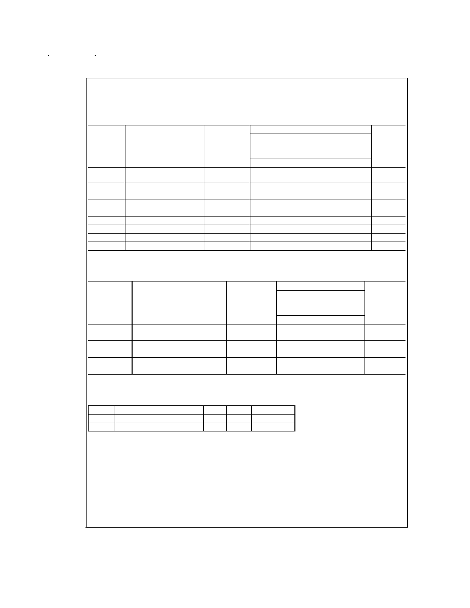
Function Table
Inputs
Internal
Outputs
Function
OE
CP
D
Q
O
N
H
H
L
NC
Z
Hold
H
H
H
NC
Z
Hold
H
N
L
L
Z
Load
H
N
H
H
Z
Load
L
N
L
L
H
Data Available
L
N
H
H
L
Data Available
L
H
L
NC
NC
No Change in Data
L
H
H
NC
NC
No Change in Data
H = HIGH Voltage Level
L = LOW Voltage Level
X = Immaterial
Z = High Impedance
N = LOW-to-HIGH Transition
NC = No Change
Pin Assignment for DIP,
and Flatpak
DS100994-3
Pin Assignment
for LCC
DS100994-4
www.national.com
2

Absolute Maximum Ratings
(Note 1)
If Military/Aerospace specified devices are required,
please contact the National Semiconductor Sales Office/
Distributors for availability and specifications.
Supply Voltage (V
CC
)
-0.5V to +7.0V
DC Input Diode Current (I
IK
)
V
I
= -0.5V
-20 mA
V
I
= V
CC
+0.5V
+20 mA
DC Input Voltage (V
I
)
-0.5V to V
CC
+0.5V
DC Output Diode Current (I
OK
)
V
O
= -0.5V
-20 mA
V
O
= V
CC
+0.5V
+20 mA
DC Output Voltage (V
O
)
-0.5V to V
CC
+0.5V
DC Output Source or Sink Current
(I
O
)
±
50 mA
DC V
CC
or Ground Current
Per Output Pin (I
CC
or I
GND
)
±
50 mA
Storage Temperature (T
STG
)
-65∞C to +150∞C
Junction Temperature (T
J
)
CDIP
175∞C
Recommended Operating
Conditions
Supply Voltage (V
CC
)
(Unless Otherwise Specified) (ACT)
4.5V to 5.5V
Input Voltage (V
I
)
0V to V
CC
Output Voltage (V
O
)
0V to V
CC
Operating Temperature (T
A
)
ACT
-55∞C to +125∞C
Minimum Input Edge Rate (
V/
t)
'ACT Devices
V
IN
from 0.8V to 2.0V
V
CC
@
4.5V, 5.5V
125 mV/ns
Note 1: Absolute maximum ratings are those values beyond which damage
to the device may occur. The databook specifications should be met, without
exception, to ensure that the system design is reliable over its power supply,
temperature, and output/input loading variables. National does not recom-
mend operation of FACT
TM
circuits outside databook specifications.
DC Characteristics for 'ACT Family Devices
54ACT
Symbol
Parameter
V
CC
T
A
=
Units
Conditions
(V)
-55∞C to +125∞C
Guaranteed Limits
V
IH
Minimum High
Level Input
Voltage
4.5
2.0
V
V
OUT
= 0.1V
5.5
2.0
or V
CC
- 0.1V
V
IL
Maximum Low
Level Input
Voltage
4.5
0.8
V
V
OUT
= 0.1V
5.5
0.8
or V
CC
- 0.1V
V
OH
Minimum High
Level
4.5
4.4
V
I
OUT
= -50 µA
5.5
5.4
(Note 2)
V
IN
= V
IL
or V
IH
4.5
3.70
V
I
OH
-24 mA
5.5
4.70
-24 mA
V
OL
Maximum Low
Level Output
Voltage
4.5
0.1
V
I
OUT
= 50 µA
5.5
0.1
(Note 2)
V
IN
= V
IL
or V
IH
4.5
0.50
V
I
OL
24 mA
5.5
0.50
24 mA
I
IN
Maximum Input
5.5
±
1.0
µA
V
I
= V
CC
, GND
Leakage Current
I
OZ
Maximum
TRI-STATE
Leakage Current
5.5
±
10.0
µA
V
I
= V
IL
, V
IH
V
O
= V
CC
, GND
I
CCT
Maximum I
CC
/Input
5.5
1.6
mA
V
I
= V
CC
- 2.1V
I
OLD
(Note 3) Minimum
Dynamic Output
Current
5.5
50
mA
V
OLD
= 1.65V
I
OHD
5.5
-50
mA
V
OHD
= 3.85V
I
CC
Maximum Quiescent
5.5
80.0
µA
V
IN
= V
CC
Supply Current
or GND
Note 2: All outputs loaded; thresholds on input associated with output under test.
www.national.com
3
DC Characteristics for 'ACT Family Devices
(Continued)
Note 3: Maximum test duration 2.0 ms, one output loaded at a time.
AC Electrical Characteristics for 'ACT Family Devices
54ACT
V
CC
T
A
= -55∞C
Symbol
Parameter
(V)
to +125∞C
Units
(Note 4)
C
L
= 50 pF
Min
Max
f
MAX
Maximum Clock
Frequency
5.0
65
ns
t
PLH
Propagation Delay
5.0
1.0
12.5
ns
CP to O
n
t
PHL
Propagation Delay
5.0
1.0
11.5
ns
CP to O
n
t
PZH
Output Enable Time
5.0
1.0
10.5
ns
t
PZL
Output Enable Time
5.0
1.0
10.5
ns
t
PHZ
Output Disable Time
5.0
1.0
12.5
ns
t
PLZ
Output Disable Time
5.0
1.0
9.5
ns
Note 4: Voltage Range 5.0 is 5.0V
±
0.5V
AC Operating Requirements for 'ACT Family Devices
54ACT
V
CC
T
A
= -55∞C
Symbol
Parameter
(V)
to +125∞C
Units
(Note 5)
C
L
= 50 pF
Guaranteed Minimum
t
s
Set-Up Time, HIGH or LOW
5.0
3.5
ns
D
n
to CP
t
h
Hold Time, HIGH or LOW
5.0
2.5
ns
D
n
to CP
t
w
CP Pulse Width
5.0
5.0
ns
HIGH or LOW
Note 5: Voltage Range 5.0 is 5.0V
±
0.5V
Capacitance
Symbol
Parameter
Typ
Units
Conditions
C
IN
Input Capacitance
4.5
pF
V
CC
= OPEN
C
PD
Power Dissipation Capacitance
40.0
pF
V
CC
= 5.0V
www.national.com
4

5