 | –≠–ª–µ–∫—Ç—Ä–æ–Ω–Ω—ã–π –∫–æ–º–ø–æ–Ω–µ–Ω—Ç: 54ACT825L | –°–∫–∞—á–∞—Ç—å:  PDF PDF  ZIP ZIP |

DS14C241
Single Supply TIA/EIA-232 4 x 5 Driver/Receiver
General Description
The DS14C241 is four driver, five receiver device which con-
forms to the TIA/EIA-232-E standard and CCITT V.28 recom-
mendations. This device eliminates
±
12V supplies by em-
ploying an internal DC≠DC converter to generate the
necessary output levels from a single +5V supply. Driver
slew rate control and receiver noise filtering have also been
internalized to eliminate the need for external slew rate con-
trol and noise filtering capacitors. With the addition of TRI-
STATE
Æ
receiver outputs and a shutdown mode, device
power consumption is kept to a minimum.
Features
n
Conforms to TIA/EIA-232-E and CCITT V.28
n
Internal DC≠DC converter
n
Operates with single +5V supply
n
Low power requirement -- I
CC
10 mA max
n
Shutdown mode -- I
CX
10 µA max
n
Internal driver slew rate control
n
Receiver noise filtering
n
Operates above 120 kbits/sec
n
TRI-STATE receiver outputs
n
Direct replacement for MAX241
Connection Diagram
Functional Diagram
TRI-STATE
Æ
is a registered trademark of National Semiconductor Corporation.
DS011281-1
Order Number DS14C241WM
See NS Package Number M28B
DS011281-2
May 1998
DS14C241
Single
Supply
TIA/EIA-23
24x5
Driver/Receiver
© 1998 National Semiconductor Corporation
DS011281
www.national.com

Absolute Maximum Ratings
(Note 1)
If Military/Aerospace specified devices are required,
please contact the National Semiconductor Sales Office/
Distributors for availability and specifications.
Supply Voltage (V
CC
)
-0.3V to +6V
V
+
Pin
(V
CC
- 0.3V) to +15V
V
-
Pin
+0.3V to -15V
Driver Input Voltage
-0.3V to (V
CC
+ 0.3V)
Driver Output Voltage
(V
+
+ 0.3V) to (V
-
- 0.3V)
Receiver Input Voltage
±
30V
Receiver Output Voltage
-0.3V to (V
CC
+ 0.3V)
Junction Temperature
+150∞C
Maximum Package Power Dissipation
@
+25∞C (Note 6)
WM Package
1520 mW
Storage Temperature Range
-65∞C to +150∞C
Lead Temperature (Soldering, 4
sec.)
+260∞C
Short Circuit Duration (D
OUT
)
continuous
ESD Rating (HBM, 1.5 k
, 100
pF)
2.0 kV
Recommended Operating
Conditions
Min
Max
Units
Supply Voltage (V
CC
)
4.5
5.5
V
Operating Free Air Temp. (T
A
)
DS14C241
0
+70
∞C
Electrical Characteristics
(Note 2)
Over recommended operating conditions, unless otherwise specified
Symbol
Parameter
Conditions
Min
Typ
Max
Units
DEVICE CHARACTERISTICS
V
+
Positive Power Supply
R
L
= 3 k
, C1≠C4 = 1.0 µF, D
IN
= 0.8V
9.0
V
V
-
Negative Power Supply
R
L
= 3 k
, C1≠C4 = 1.0 µF, D
IN
= 2.0V
-8.0
V
I
CC
Supply Current (V
CC
)
No Load
8.5
10
mA
I
CX
Supply Current Shutdown
R
L
= 3 k
, SD = V
CC
1.0
10
µA
V
IH
High Level Enable Voltage
SD
2.4
V
CC
V
V
IL
Low Level Enable Voltage
GND
0.8
V
I
IH
High Level Enable Current
-10
+10
µA
I
IL
Low Level Enable Current
-10
+10
µA
DRIVER CHARACTERISTICS
V
IH
High Level Input Voltage
D
IN
2.0
V
CC
V
V
IL
Low Level Input Voltage
GND
0.8
V
I
IH
High Level Input Current
V
IN
2.0V
-10
+10
µA
I
IL
Low Level Input Current
V
IN
0.8V
-10
+10
µA
V
OH
High Level Output Voltage
R
L
= 3 k
5.0
7.5
V
V
OL
Low Level Output Voltage
-6.5
-5.0
V
I
OS
+
Output High Short Circuit Current
V
O
= 0V, V
IN
= 0.8V
-30
-15
-5.0
mA
I
OS
-
Output Low Short Circuit Current
V
O
= 0V, V
IN
= 2.0V
5.0
12
30
mA
R
O
Output Resistance
-2V
V
O
+2V, V
CC
= GND = 0V
300
RECEIVER CHARACTERISTICS
V
TH
Input High Threshold Voltage
1.9
2.4
V
V
TL
Input Low Threshold Voltage
0.8
1.5
V
V
HY
Hysteresis
0.2
0.4
1.0
V
R
IN
Input Resistance
3.0
4.5
7.0
k
I
IN
Input Current
V
IN
= +15V
2.14
3.8
5.0
mA
V
IN
= +3V
0.43
0.6
1.0
mA
V
IN
= -3V
-1.0
-0.6
-0.43
mA
V
IN
= -15V
-5.0
-3.8
-2.14
mA
V
OH
High Level Output Voltage
V
IN
= -3V, I
O
= -3.2 mA
3.5
4.6
V
V
IN
= -3V, I
O
= -20 µA
4.0
4.9
V
V
OL
Low Level Output Voltage
V
IN
= +3V, I
O
= +2.0 mA
0.25
0.4
V
www.national.com
2

Electrical Characteristics
(Note 2) (Continued)
Over recommended operating conditions, unless otherwise specified
Symbol
Parameter
Conditions
Min
Typ
Max
Units
RECEIVER CHARACTERISTICS
V
IH
High Level Input Voltage
EN
2.0
V
CC
V
V
IL
Low Level Input Voltage
GND
0.8
V
I
IH
High Level Input Current
V
IN
2.0V
-10
+10
µA
I
IL
Low Level Input Current
V
IN
0.8V
-10
+10
µA
I
OZ
Output Leakage Current
EN = V
CC
, 0V
R
OUT
V
CC
-10
+10
µA
Switching Characteristics
(Note 4)
Over recommended operating conditions, unless otherwise specified
Symbol
Parameter
Conditions
Min
Typ
Max
Units
DRIVER CHARACTERISTICS
t
PLH
Propagation Delay LOW to HIGH
R
L
= 3 k
0.7
4.0
µs
t
PHL
Propagation Delay HIGH to LOW
C
L
= 50 pF
0.6
4.0
µs
t
SK
Skew |t
PLH
≠t
PHL
|
(
Figures 1, 2)
0.1
1.0
µs
SR1
Output Slew Rate
R
L
= 3 k
to 7 k
, C
L
= 50 pF
4.0
15
30
V/µs
SR2
Output Slew Rate
R
L
= 3 k
, C
L
= 2500 pF
3.0
5.0
V/µs
RECEIVER CHARACTERISTICS
t
PLH
Propagation Delay LOW to HIGH
Input Pulse Width
>
10 µs
C
L
= 50 pF
(
Figures 3, 4)
2.0
6.5
µs
t
PHL
Propagation Delay HIGH to LOW
2.8
6.5
µs
t
SK
Skew |t
PLH
≠t
PHL
|
0.8
2.0
µs
t
PLZ
(
Figures 5, 7)
0.1
2.0
µs
t
PZL
0.6
2.0
µs
t
PHZ
(
Figures 5, 6)
0.2
2.0
µs
t
PZH
0.6
2.0
µs
t
NW
Noise Pulse Width Rejected
(
Figures 3, 4)
2.5
1.0
µs
Note 1: "Absolute Maximum Ratings" are those values beyond which the safety of the device cannot be guaranteed. They are not meant to imply that the devices
should be operated at these limits. The tables of "Electrical Characteristics" specify conditions for device operation.
Note 2: Current into device pins is defined as positive. Current out of device pins is defined as negative. All voltages are referenced to ground unless otherwise speci-
fied.
Note 3: I
OS
+ and I
OS
- values are for one output at a time. If more than one output is shorted simultaneously, the device power dissipation may be exceeded.
Note 4: Receiver AC input waveform for test purposes: t
r
= t
f
= 200 ns, V
IH
= 3V, V
IL
= -3V, f = 64 kHz (128 kbits/sec). Driver AC input waveform for test purposes:
t
r
= t
f
10 ns, V
IH
= 3V, V
IL
= 0V, f = 64 kHz (128 kbits/sec).
Note 5: All typicals are given for V
CC
= 5.0V and T
A
= +25∞C.
Note 6: Ratings apply to ambient temperature at +25∞C. Above this temperature derate: WM package 14.3 mW/∞C.
Parameter Measurement Information
DS011281-4
FIGURE 1. Driver Load Circuit
www.national.com
3

Parameter Measurement Information
(Continued)
DS011281-5
FIGURE 2. Driver Switching Waveform
DS011281-6
FIGURE 3. Receiver Load Circuit
DS011281-7
FIGURE 4. Receiver Propagation Delays and Noise Rejection
DS011281-8
FIGURE 5. Receiver Disable Load Circuit
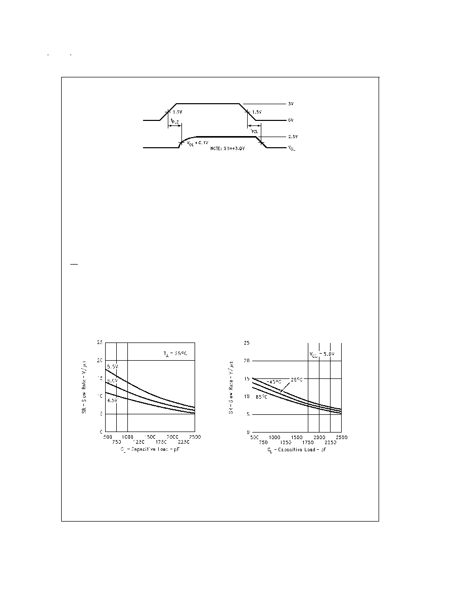
DS011281-9
FIGURE 6. Receiver TRI-STATE Timing (t
PHZ
, t
PZH
)
www.national.com
4
Parameter Measurement Information
(Continued)
Pin Descriptions
V
CC
(pin 11) -- Power supply pin for the device,
+5V (
±
10%).
V
+
(pin 13) -- Positive supply for TIA/EIA-232-E drivers.
Recommended external capacitor: C4 = 1.0 µF (6.3V). This
supply is not intended to be loaded externally.
V
-
(pin 17) -- Negative supply for TIA/EIA-232-E drivers.
Recommended external capacitor: C3 = 1.0 µF (16V). This
supply is not intended to be loaded externally.
C1
+
, C1
-
(pins 12 and 14) -- External capacitor connection
pins. Recommended capacitor -- 1.0 µF (6.3V).
C2
+
, C2
-
(pins 15 and 16) -- External capacitor connection
pins. Recommended capacitor -- 1.0 µF (16V).
EN (pin 24) -- Controls the Receiver output TRI-STATE Cir-
cuit. A HIGH level on this pin will disable the Receiver Out-
put.
SHUTDOWN (SD) (pin 25) -- A High on the SHUTDOWN
pin will lower the total I
CC
current to less than 10 µA. Provid-
ing a low power state.
D
IN
1≠4 (pins 7, 6, 20 and 21) -- Driver input pins are TTL/
CMOS compatible. Inputs of unused drivers may be left
open, an internal pull-up resistor (500 k
minimum, typically
5 M
) pulls input to V
CC
. Output will be LOW for open inputs.
D
OUT
1≠4 (pins 2, 3, 1 and 28) -- Driver output pins con-
form to TIA/EIA-232-E levels.
R
IN
1≠5 (pins 9, 4, 27, 23 and 18) -- Receiver input pins ac-
cept TIA/EIA-232-E input voltages (
±
15V). Receivers fea-
ture a noise filter and guaranteed hysteresis of 200 mV. Un-
used receiver input pins may be left open. Internal input
resistor (5 k
) pulls input LOW, providing a failsafe HIGH
output.
R
OUT
1≠5 (pins 8, 5, 26, 22 and 19) -- Receiver output pins
are TTL/CMOS compatible. Receiver output HIGH voltage is
specified for both CMOS and TTL load conditions.
GND (pin 10) -- Ground pin.
Typical Performance Characteristics
DS011281-10
FIGURE 7. Receiver TRI-STATE Timing (t
PLZ
, t
PZL
)
Slew Rate vs Cap. Load vs V
CC
(Four Drivers)
DS011281-11
Slew Rate vs Temperature vs
Cap. Load (Four Drivers Switching)
DS011281-12
www.national.com
5