54ACTQ16373
16-Bit Transparent Latch with TRI-STATE
Æ
Outputs
General Description
The 'ACTQ16373 contains sixteen non-inverting latches with
TRI-STATE outputs and is intended for bus oriented applica-
tions. The device is byte controlled. The flip-flops appear
transparent to the data when the Latch Enable (LE) is HIGH.
When LE is low, the data that meets the setup time is
latched. Data appears on the bus when the Output Enable
(OE) is LOW. When OE is HIGH, the outputs are in high Z
state. The 'ACTQ16373 utilizes NSC Quiet Series technol-
ogy to guarantee quiet output switching and improved dy-
namic threshold performance. FACT Quiet Series
TM
features
GTO
TM
output control for superior performance.
Features
n
Utilizes NSC FACT Quiet Series technology
n
Guaranteed simultaneous switching noise level and
dynamic threshold performance
n
Separate control logic for each byte
n
16-bit version of the 'ACTQ373
n
Outputs source/sink 24 mA
n
Standard Microcircuit Drawing (SMD) 5962-9561801
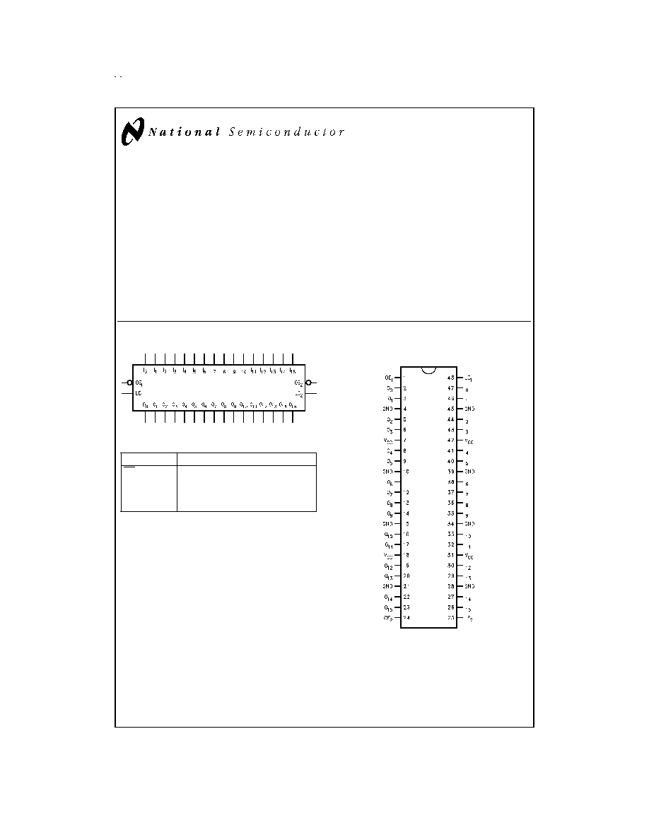
Logic Symbol
Pin Description
Pin Names
Description
OE
n
Output Enable Input (Active Low)
LE
n
Latch Enable Input
I
0
≠I
15
Inputs
O
0
≠O
15
Outputs
Connection Diagram
TRI-STATE
Æ
is a registered trademark of National Semiconductor Corporation.
GTO
TM
is a trademarks of National Semiconductor Corporation.
FACT
TM
and FACT Quiet Series
TM
are trademarks of Fairchild Semiconductor Corporation.
DS010934-1
Pin Assignment for CERPAK
DS010934-2
September 1998
54ACTQ16373
16-Bit
T
ransparent
Latch
with
TRI-ST
A
T
E
Outputs
© 1998 National Semiconductor Corporation
DS010934
www.national.com
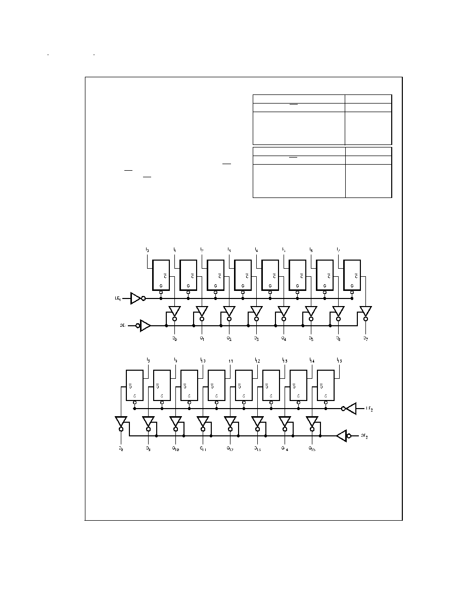
Functional Description
The 'ACTQ16373 contains sixteen D-type latches with
TRI-STATE standard outputs. The device is byte controlled
with each byte functioning identically, but independent of the
other. Control pins can be shorted together to obtain full
16-bit operation. The following description applies to each
byte. When the Latch Enable (LE
n
) input is HIGH, data on
the D
n
enters the latches. In this condition the latches are
transparent, i.e., a latch output will change states each time
its D input changes. When LE
n
is LOW, the latches store in-
formation that was present on the D inputs a setup time pre-
ceding the HIGH-to-LOW transition of LE
n
. The TRI-STATE
standard outputs are controlled by the Output Enable (OE
n
)
input. When OE
n
is LOW, the standard outputs are in the
2-state mode. When OE
n
is HIGH, the standard outputs are
in the high impedance mode but this does not interfere with
entering new data into the latches.
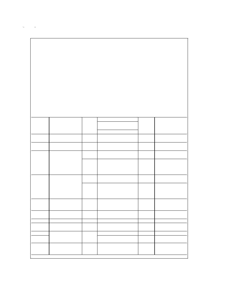
Truth Table
Inputs
Outputs
LE
1
OE
1
I
0
≠I
7
O
0
≠O
7
X
H
X
Z
H
L
L
L
H
L
H
H
L
L
X
(Previous)
Inputs
Outputs
LE
2
OE
2
I
8
≠I
15
O
8
≠O
15
X
H
X
Z
H
L
L
L
H
L
H
H
L
L
X
(Previous)
H = High Voltage Level
L = Low Voltage Level
X = Immaterial
Z = High Impedance
Previous = previous output prior to HIGH to LOW transition of LE
Logic Diagrams
DS010934-3
DS010934-4
www.national.com
2
Absolute Maximum Ratings
(Note 1)
If Military/Aerospace specified devices are required,
please contact the National Semiconductor Sales Office/
Distributors for availability and specifications.
Supply Voltage (V
CC
)
-0.5V to +7.0V
DC Input Diode Current (I
IK
)
V
I
= -0.5V
-20 mA
V
I
= V
CC
+ 0.5V
+20 mA
DC Output Diode Current (I
OK
)
V
O
= -0.5V
-20 mA
V
O
= V
CC
+ 0.5V
+20 mA
DC Output Voltage (V
O
)
-0.5V to V
CC
+ 0.5V
DC Output Source/Sink Current (I
O
)
+50 mA
DC V
CC
or Ground Current
+50 mA
per Output Pin
Junction Temperature
CDIP
+175∞C
Storage Temperature
-65∞C to +150∞C
Recommended Operating
Conditions
Supply Voltage (V
CC
)
'ACTQ
4.5V to 5.5V
Input Voltage (V
I
)
0V to V
CC
Output Voltage (V
O
)
0V to V
CC
Operating Temperature (T
A
)
54ACTQ
-55∞C to +125∞C
Minimum Input Edge Rate (dV/dt)
'ACTQ Devices
125 mV/ns
V
IN
from 0.8V to 2.0V
V
CC
@
4.5V, 5.5V
Note 1: Absolute maximum ratings are those values beyond which damage
to the device may occur. The databook specifications should be met, without
exception to ensure that the system design is reliable over its power supply,
temperature, and output/input loading variables. National does not recom-
mend operation of FACT
TM
circuits outside databook specifications.
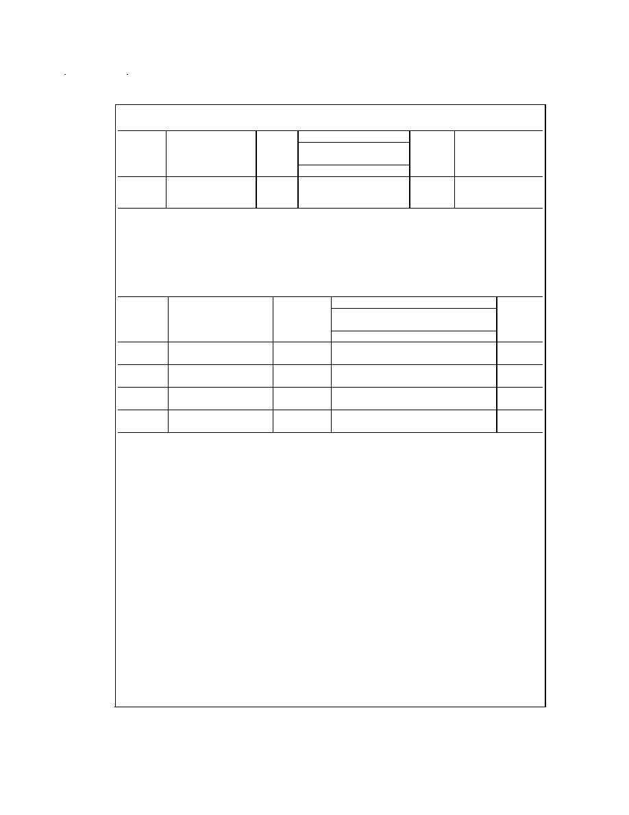
DC Electrical Characteristics for 'ACTQ Family Devices
Symbol
Parameter
V
CC
(V)
54ACTQ
Units
Conditions
T
A
=
-55∞C to +125∞C
Guaranteed Limits
V
IH
Minimum High
4.5
2.0
V
V
OUT
= 0.1V
Input Voltage
5.5
2.0
or V
CC
- 0.1V
V
IL
Maximum Low
4.5
0.8
V
V
OUT
= 0.1V
Input Voltage
5.5
0.8
or V
CC
- 0.1V
V
OH
Minimum High
4.5
4.4
V
I
OUT
= -50 µA
Output Voltage
5.5
5.4
(Note 2)
V
IN
= V
IL
or V
IH
4.5
3.70
V
I
OH
= -24 mA
5.5
4.70
I
OH
= -24 mA
V
OL
Maximum Low
4.5
0.1
V
I
OUT
= 50 µA
Output Voltage
5.5
0.1
(Note 2)
V
IN
= V
IL
or V
IH
4.5
0.50
V
I
OL
= 24 mA
5.5
0.50
I
OL
= 24 mA
I
OZ
Maximum
5.5
±
10.0
µA
V
I
= V
IL
, V
IH
TRI-STATE
Leakage Current
V
O
= V
CC
, GND
I
IN
Maximum Input
5.5
±
1.0
µA
V
I
= V
CC
, GND
Leakage Current
I
CCT
Maximum I
CC
/Input
5.5
1.6
mA
V
I
= V
CC
- 2.1V
I
CC
Max Quiescent
5.5
160.0
µA
V
IN
= V
CC
or GND
Supply Current
(Note 7)
I
OLD
Minimum Dynamic
5.5
50
mA
V
OLD
= 1.65V Max
I
OHD
Output Current
(Note 3)
50
mA
V
OHD
= 3.85V Min
V
OLP
Quiet Output
5.0
0.8
V
Maximum Dynamic
V
OL
(Notes 4, 5)
www.national.com
3
DC Electrical Characteristics for 'ACTQ Family Devices
(Continued)
Symbol
Parameter
V
CC
(V)
54ACTQ
Units
Conditions
T
A
=
-55∞C to +125∞C
Guaranteed Limits
V
OLV
Quiet Output
5.0
-0.8
V
Minimum Dynamic
V
OL
(Notes 4, 5)
Note 2: All outputs loaded; thesholds associated with output unders test.
Note 3: Maximum test duration 2.0 ms; one output loaded at a time.
Note 4: Maximum number of outputs that can switch simultaneously is n. (n - 1) outputs are switched LOW and one output held LOW.
Note 5: Maximum number of outputs that can switch simultaneously is n. (n - 1) outputs are switched HIGH and one output held HIGH.
Note 6: Max number of data inputs (n) switching, (n - 1) input switching 0V to 3V ('ACTQ). Input under test switching 3V to threshold (V
ILD
)
Note 7: I
CC
for 54ACTQ
@
25∞C is indentical to 74ACTQ
@
25∞C.
AC Electrical Characteristics:
Symbol
Parameter
V
CC
(V)
(Note 8)
54ACTQ
Units
T
A
= -55∞C to+125∞C
C
L
= 50 pF
Min
Max
t
PLH
Propagation Delay
5.0
3.0
10.5
ns
t
PHL
D
n
to O
n
3.0
10.0
t
PLH
Propagation Delay
5.0
3.0
11.0
ns
t
PHL
LE to O
n
3.0
10.0
t
PZH
Output Enable
5.0
2.5
10.0
ns
t
PZL
Delay
2.5
11.0
t
PHZ
Output Disable
5.0
2.0
9.0
ns
t
PLZ
Delay
2.0
9.0
Note 8: Voltage Range 5.0 is 5.0V
±
0.5V.
www.national.com
4

AC Operating Requirements:
Symbol
Parameter
V
CC
(V)
(Note 9)
54ACTQ
Units
-55∞C to +125∞C
50 pF
Guaranteed Minimum
t
S
Setup Time, HIGH or
5.0
3.0
ns
LOW, Input to Clock
t
h
Hold time, High or
5.0
1.5
ns
LOW, Input to Clock
t
w
CS Pulse Width,
5.0
4.0
ns
HIGH or LOW
Note 9: Voltage Range 5.0 is 5.0V
±
0.5V
Capacitance
Symbol
Parameter
Typ
Units
Conditions
C
IN
Input Capacitance
4.5
pF
V
CC
= 5.0V
C
PD
Power Dissipation
95
pF
V
CC
= 5.0V
www.national.com
5