
54ACTQ273
Quiet Series Octal D Flip-Flop
General Description
The ACTQ273 has eight edge-triggered D-type flip-flops with
individual D inputs and Q outputs. The common buffered
Clock (CP) and Master Reset (MR) input load and reset
(clear) all flip-flops simultaneously.
The register is fully edge-triggered. The state of each D in-
put, one setup time before the LOW-to-HIGH clock transi-
tion, is transferred to the corresponding flip-flop's Q output.
All outputs will be forced LOW independently of Clock or
Data inputs by a LOW voltage level on the MR input. The de-
vice is useful for applications where the true output only is re-
quired and the Clock and Master Reset are common to all
storage elements.
The ACTQ utilizes NSC Quiet Series technology to guaran-
tee quiet output switching and improved dynamic threshold
performance. FACT Quiet Series
TM
features GTO
TM
output
control and undershoot corrector in addition to a split ground
bus for superior performance.
Features
n
I
CC
reduced by 50%
n
Guaranteed simultaneous switching noise level and
dynamic threshold performance
n
Improved latch-up immunity
n
Buffered common clock and asynchronous master reset
n
Outputs source/sink 24 mA
n
Faster prop delays than the standard 'AC/'ACT273
n
4 kV minimum ESD immunity
n
Standard Microcircuit Drawing (SMD)
5962-89735
Logic Symbols
Pin Names
Description
D
0
�D
7
Data Inputs
MR
Master Reset
CP
Clock Pulse Input
Q
0
�Q
7
Data Outputs
GTO
TM
is a trademark of National Semiconductor Corporation.
FACT
�
is a registered trademark of Fairchild Semiconductor Corporation.
FACT Quiet Series
TM
is a trademark of Fairchild Semiconductor Corporation.
DS100240-1
IEEE/IEC
DS100240-2
August 1998
54ACTQ273
Quiet
Series
Octal
D
Flip-Flop
� 1998 National Semiconductor Corporation
DS100240
www.national.com
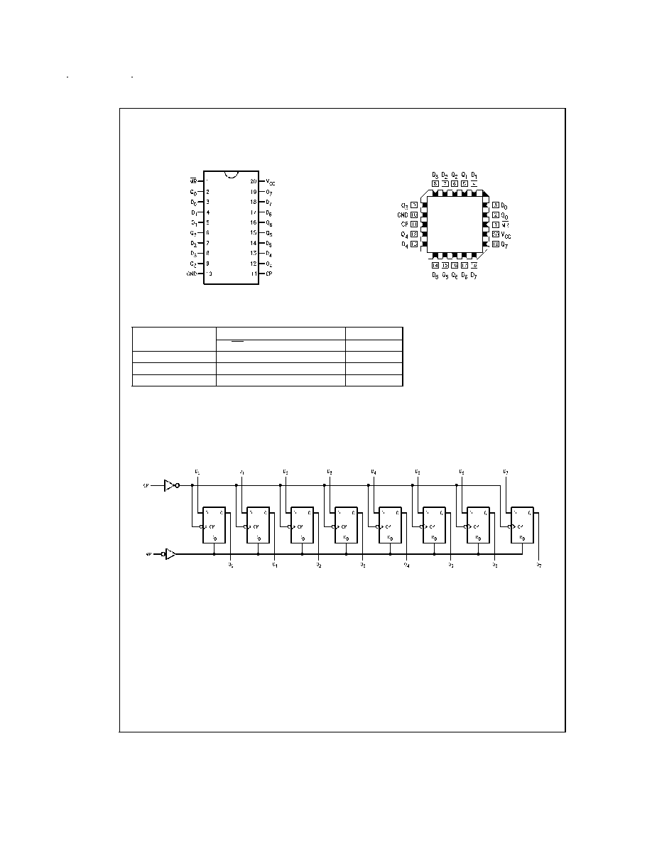
Connection Diagrams
Mode Select-Function Table
Operating Mode
Inputs
Outputs
MR
CP
D
n
Q
n
Reset (Clear)
L
X
X
L
Load "1"
H
N
H
H
Load "0"
H
N
L
L
Note 1: H = HIGH Voltage Level
Note 2: L = LOW Voltage Level
Note 3: X = Immaterial
Note 4:
N
= LOW-to-HIGH Transition
Logic Diagram
Pin Assignment
for DIP and Flatpak
DS100240-3
Pin Assignment
for LCC
DS100240-4
DS100240-5
Please note that this diagram is provided only for the understanding of logic operations and should not be used to estimate propagation delays.
www.national.com
2

Absolute Maximum Ratings
(Note 5)
If Military/Aerospace specified devices are required,
please contact the National Semiconductor Sales Office/
Distributors for availability and specifications.
Supply Voltage (V
CC
)
-0.5V to +7.0V
DC Input Diode Current (I
IK
)
V
I
= -0.5V
-20 mA
V
I
= V
CC
+ 0.5V
+20 mA
DC Input Voltage (V
I
)
-0.5V to V
CC
+ 0.5V
DC Output Diode Current (I
OK
)
V
O
= -0.5V
-20 mA
V
O
= V
CC
+ 0.5V
+20 mA
DC Output Voltage (V
O
)
-0.5V to V
CC
+ 0.5V
DC Output Source
or Sink Current (I
O
)
�
50 mA
DC V
CC
or Ground Current
per Output Pin (I
CC
or I
GND
)
�
50 mA
Storage Temperature (T
STG
)
-65�C to +150�C
DC Latch-up Source or
Sink Current
�
300 mA
Junction Temperature (T
J
)
CDIP
175�C
Recommended Operating
Conditions
Supply Voltage (V
CC
)
'ACTQ
4.5V to 5.5V
Input Voltage (V
I
)
0V to V
CC
Output Voltage (V
O
)
0V to V
CC
Operating Temperature (T
A
)
54ACTQ
-55�C to +125�C
Minimum Input Edge Rate
V/
t
'ACTQ Devices
V
IN
from 0.8V to 2.0V
V
CC
@
4.5V, 5.5V
125 mV/ns
Note 5: Absolute maximum ratings are those values beyond which damage
to the device may occur. The databook specifications should be met, without
exception, to ensure that the system design is reliable over its power supply,
temperature, and output/input loading variables. National does not recom-
mend operation of FACT
�
circuits outside databook specifications.
Note 6: All commercial packaging is not recommended for applications re-
quiring greater than 2000 temperature cycles from -40�C to +125�C.
DC Characteristics for 'ACTQ Family Devices
54ACTQ
Symbol
Parameter
V
CC
T
A
= -55�C
Units
Conditions
(V)
to +125�C
Guaranteed Limits
V
IH
Minimum High Level
4.5
2.0
V
V
OUT
= 0.1V
Input Voltage
5.5
2.0
or V
CC
- 0.1V
V
IL
Maximum Low Level
4.5
0.8
V
V
OUT
= 0.1V
Input Voltage
5.5
0.8
or V
CC
- 0.1V
V
OH
Minimum High Level
4.5
4.4
V
I
OUT
= -50 �A
Output Voltage
5.5
5.4
(Note 7)
V
IN
= V
IL
or V
IH
4.5
3.7
V
I
OH
= -24 mA
5.5
4.7
I
OH
= -24 mA
V
OL
Maximum Low Level
4.5
0.1
V
I
OUT
= 50 �A
Output Voltage
5.5
0.1
(Note 7)
V
IN
= V
IL
or V
IH
4.5
0.50
V
I
OL
= 24 mA
5.5
0.50
I
OL
= 24 mA
I
IN
Maximum Input
5.5
�
1.0
�A
V
I
= V
CC
, GND
Leakage Current
I
CCT
Maximum
5.5
1.6
mA
V
I
= V
CC
- 2.1V
I
CC
/Input
I
OLD
Minimum Dynamic
Output Current (Note 8)
5.5
50
mA
V
OLD
= 1.65V Max
I
OHD
5.5
-50
mA
V
OHD
= 3.85V Min
I
CC
Maximum Quiescent
5.5
80.0
�A
V
IN
= V
CC
Supply Current
or GND (Note 9)
www.national.com
3

DC Characteristics for 'ACTQ Family Devices
(Continued)
54ACTQ
Symbol
Parameter
V
CC
T
A
= -55�C
Units
Conditions
(V)
to +125�C
Guaranteed Limits
V
OLP
Quiet Output
5.0
1.5
V
(Note 10)
Maximum Dynamic V
OL
V
OLV
Quiet Output
5.0
-1.2
V
(Note 10)
Minimum Dynamic V
OL
Note 7: All outputs loaded; thresholds on input associated with output under test.
Note 8: Maximum test duration 2.0 ms, one output loaded at a time.
Note 9: I
CC
for 54ACTQ
@
25�C is identical to 74ACTQ
@
25�C.
Note 10: Max number of outputs defined as (n). n - 1 Data inputs are driven 0V to 3V; one output
@
GND.
Note 11: Max number of Data Inputs (n) switching. (n - 1) Inputs switching 0V to 3V ('ACTQ). Input-under-test switching: 3V to threshold (V
ILD
), 0V to threshold
(V
IHD
) f = 1 MHz.
AC Electrical Characteristics
54ACTQ
V
CC
T
A
= -55�C
Fig.
Symbol
Parameter
(V)
to +125�C
Units
No.
(Note 12)
C
L
= 50 pF
Min
Max
f
max
Maximum Clock
5.0
85
MHz
Frequency
t
PHL
,
t
PLH
Propagation Delay
Clock to Output
5.0
1.5
10.0
ns
Figure 4
t
PHL
Propagation Delay
5.0
1.5
11.0
ns
Figure 4
MR to Output
Note 12:
Voltage Range 5.0 is 5.0V
�
0.5V.
AC Operating Requirements
54ACTQ
V
CC
T
A
= -55�C
Fig.
Symbol
Parameter
(V)
to +125�C
Units
No.
(Note 13)
C
L
= 50 pF
Guaranteed Minimum
t
s
Setup Time, HIGH
or LOW
5.0
5.0
ns
Figure 6
Data to CP
t
h
Hold Time, HIGH or
LOW
5.0
2.0
ns
Figure 6
Data to CP
t
w
Clock Pulse Width
5.0
5.0
ns
Figure 5
HIGH or LOW
t
w
MR Pulse Width
5.0
5.0
ns
Figure 5
HIGH or LOW
t
rec
Recovery Time
5.0
4.0
ns
Figure 6
MR to CP
Note 13: Voltage Range 5.0 is 5.0V
�
0.5V
www.national.com
4
Capacitance
Symbol
Parameter
Typ
Units
Conditions
C
IN
Input Capacitance
4.5
pF
V
CC
= OPEN
C
PD
Power Dissipation
40.0
pF
V
CC
= 5.0V
Capacitance
AC Loading
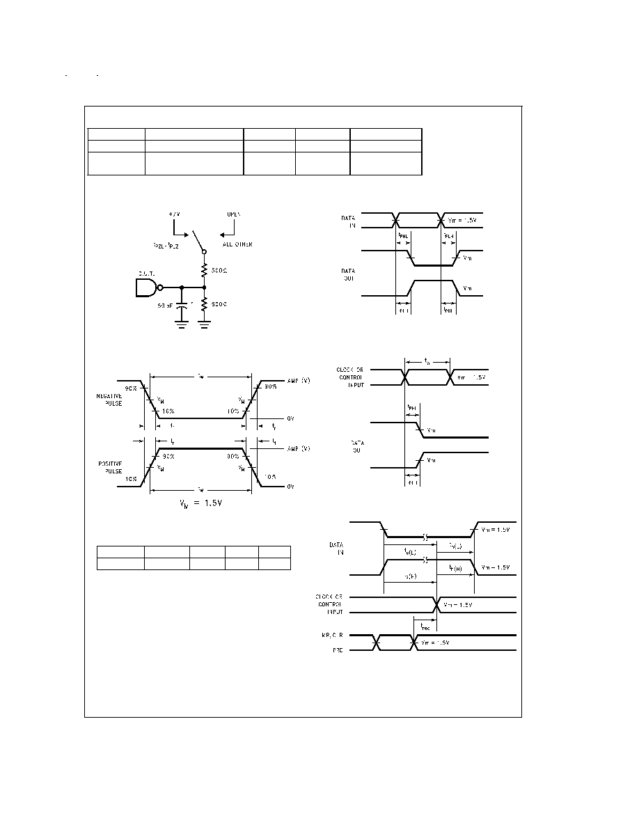
AC Waveforms
DS100240-31
*Includes jig and probe capacitance
FIGURE 1. Standard AC Test Load
DS100240-32
FIGURE 2. Test Input Signal Levels
Amplitude
Rep.Rate
t
w
t
r
t
f
3.0V
1 MHz
500 ns
2.5 ns
2.5 ns
FIGURE 3. Test Input Signal Requirements
DS100240-33
FIGURE 4. Propogation Delay Waveforms for Inverting
and Non-Inverting Functions
DS100240-34
FIGURE 5. Propogation Delay, Pulse Width Waveforms
DS100240-35
FIGURE 6. Setup Time, Hold Time and
Recovery Time Waveforms
www.national.com
5