
TL F 9481
54F74F151A
8-Input
Multiplexer
November 1994
54F 74F151A
8-Input Multiplexer
General Description
The 'F151A is a high-speed 8-input digital multiplexer It pro-
vides in one package the ability to select one line of data
from up to eight sources The 'F151A can be used as a
universal function generator to generate any logic function
of four variables Both assertion and negation outputs are
provided
Commercial
Military
Package
Package Description
Number
74F151APC
N16E
16-Lead (0 300 Wide) Molded Dual-In-Line
54F151ADM (Note 2)
J16A
16-Lead Ceramic Dual-In-Line
74F151ASC (Note 1)
M16A
16-Lead (0 150 Wide) Molded Small Outline JEDEC
74F151ASJ (Note 1)
M16D
16-Lead (0 300 Wide) Molded Small Outline EIAJ
54F151AFM (Note 2)
W16A
16-Lead Cerpack
54F151ALM (Note 2)
E20A
20-Lead Ceramic Leadless Chip Carrier Type C
Note 1
Devices also available in 13
reel Use suffix
e
SCX and SJX
Note 2
Military grade device with environmental and burn-in processing Use suffix
e
DQMB FMQB and LMQB
Logic Symbols
Connection Diagrams
TL F 9481 � 3
IEEE IEC
TL F 9481 � 5
Pin Assignment for DIP
SOIC and Flatpak
TL F 9481 � 1
Pin Assignment
for LCC
TL F 9481 � 2
TRI-STATE
is a registered trademark of National Semiconductor Corporation
C1995 National Semiconductor Corporation
RRD-B30M115 Printed in U S A
Unit Loading Fan Out
54F 74F
Pin Names
Description
U L
Input I
IH
I
IL
HIGH LOW
Output I
OH
I
OL
I
0
� I
7
Data Inputs
1 0 1 0
20 mA
b
0 6 mA
S
0
� S
2
Select Inputs
1 0 1 0
20 mA
b
0 6 mA
E
Enable Input (Active LOW)
1 0 1 0
20 mA
b
0 6 mA
Z
Data Output
50 33 3
b
1 mA 20 mA
Z
Inverted Data Output
50 33 3
b
1 mA 20 mA
Functional Description
The 'F151A is a logic implementation of a single pole 8-po-
sition switch with the switch position controlled by the state
of three Select inputs S
0
S
1
S
2
Both assertion and nega-
tion outputs are provided The Enable input (E) is active
LOW When it is not activated the negation output is HIGH
and the assertion output is LOW regardless of all other in-
puts The logic function provided at the output is
Z
e
E
(I
0
S
2
S
1
S
0
a
I
1
S
2
S
1
S
0
a
I
2
S
2
S
1
S
0
a
I
3
S
2
S
1
S
0
a
I
4
S
2
S
1
S
0
a
I
5
S
2
S
1
S
0
a
I
6
S
2
S
1
S
0
a
I
7
S
2
S
1
S
0
)
The 'F151A provides the ability in one package to select
from eight sources of data or control information By proper
manipulation of the inputs the 'F151A can provide any logic
function of four variables and its negation
Truth Table
Inputs
Outputs
E
S
2
S
1
S
0
Z
Z
H
X
X
X
H
L
L
L
L
L
I
0
I
0
L
L
L
H
I
1
I
1
L
L
H
L
I
2
I
2
L
L
H
H
I
3
I
3
L
H
L
L
I
4
I
4
L
H
L
H
I
5
I
5
L
H
H
L
I
6
I
6
L
H
H
H
I
7
I
7
H
e
HIGH Voltage Level
L
e
LOW Voltage Level
X
e
Immaterial
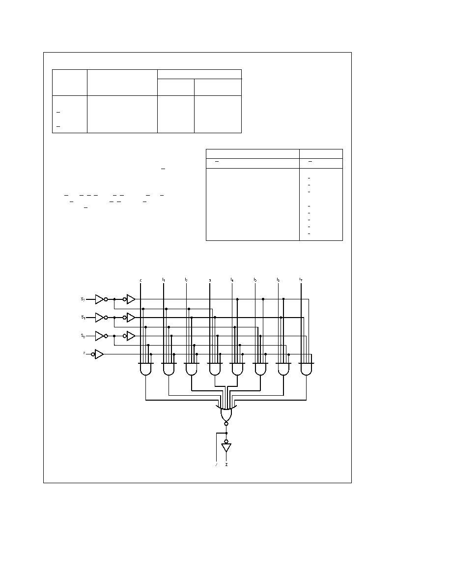
Logic Diagram
TL F 9481 � 4
Please note that this diagram is provided only for the understanding of logic operations and should not be used to estimate propagation delays
2

Absolute Maximum Ratings
(Note 1)
If Military Aerospace specified devices are required
please contact the National Semiconductor Sales
Office Distributors for availability and specifications
Storage Temperature
b
65 C to
a
150 C
Ambient Temperature under Bias
b
55 C to
a
125 C
Junction Temperature under Bias
b
55 C to
a
175 C
Plastic
b
55 C to
a
150 C
V
CC
Pin Potential to
Ground Pin
b
0 5V to
a
7 0V
Input Voltage (Note 2)
b
0 5V to
a
7 0V
Input Current (Note 2)
b
30 mA to
a
5 0 mA
Voltage Applied to Output
in HIGH State (with V
CC
e
0V)
Standard Output
b
0 5V to V
CC
TRI-STATE Output
b
0 5V to
a
5 5V
Current Applied to Output
in LOW State (Max)
twice the rated I
OL
(mA)
Note 1
Absolute maximum ratings are values beyond which the device may
be damaged or have its useful life impaired Functional operation under
these conditions is not implied
Note 2
Either voltage limit or current limit is sufficient to protect inputs
Recommended Operating
Conditions
Free Air Ambient Temperature
Military
b
55 C to
a
125 C
Commercial
0 C to
a
70 C
Supply Voltage
Military
a
4 5V to
a
5 5V
Commercial
a
4 5V to
a
5 5V
DC Electrical Characteristics
Symbol
Parameter
54F 74F
Units
V
CC
Conditions
Min
Typ
Max
V
IH
Input HIGH Voltage
2 0
V
Recognized as a HIGH Signal
V
IL
Input LOW Voltage
0 8
V
Recognized as a LOW Signal
V
CD
Input Clamp Diode Voltage
b
1 2
V
Min
I
IN
e b
18 mA
V
OH
Output HIGH
54F 10% V
CC
2 5
I
OH
e b
1 mA
Voltage
74F 10% V
CC
2 5
V
Min
I
OH
e b
1 mA
74F 5% V
CC
2 7
I
OH
e b
1 mA
V
OL
Output LOW
54F 10% V
CC
0 5
V
Min
I
OL
e
20 mA
Voltage
74F 10% V
CC
0 5
I
OL
e
20 mA
I
IH
Input HIGH
54F
20 0
m
A
Max
V
IN
e
2 7V
Current
74F
5 0
I
BVI
Input HIGH Current
54F
100
m
A
Max
V
IN
e
7 0V
Breakdown Test
74F
7 0
I
CEX
Output HIGH
54F
250
m
A
Max
V
OUT
e
V
CC
Leakage Current
74F
50
V
ID
Input Leakage
74F
4 75
V
0 0
I
ID
e
1 9 mA
Test
All Other Pins Grounded
I
OD
Output Leakage
74F
3 75
m
A
0 0
V
IOD
e
150 mV
Circuit Current
All Other Pins Grounded
I
IL
Input LOW Current
b
0 6
mA
Max
V
IN
e
0 5V
I
OS
Output Short-Circuit Current
b
60
b
150
mA
Max
V
OUT
e
0V
I
CC
Power Supply Current
13 5
21 0
mA
Max
V
O
e
HIGH
3

AC Electrical Characteristics
74F
54F
74F
T
A
e a
25 C
T
A
V
CC
e
Mil
T
A
V
CC
e
Com
Symbol
Parameter
V
CC
e a
5 0V
C
L
e
50 pF
C
L
e
50 pF
Units
C
L
e
50 pF
Min
Typ
Max
Min
Max
Min
Max
t
PLH
Propagation Delay
4 0
6 2
9 0
3 5
11 5
3 5
9 5
ns
t
PHL
S
n
to Z
3 2
5 2
7 5
3 0
8 0
3 2
7 5
t
PLH
Propagation Delay
4 5
7 5
10 5
4 5
13 5
4 5
12 0
ns
t
PHL
S
n
to Z
4 0
6 2
9 0
4 0
9 5
4 0
9 0
t
PLH
Propagation Delay
3 0
4 7
6 1
3 0
7 5
3 0
7 0
ns
t
PHL
E to Z
3 0
4 4
6 0
2 5
6 5
2 5
6 0
t
PLH
Propagation Delay
5 0
7 0
9 5
4 0
12 0
4 0
10 5
ns
t
PHL
E to Z
3 5
5 3
7 0
3 0
8 0
3 0
7 5
t
PLH
Propagation Delay
3 0
4 8
6 5
2 5
7 5
3 0
7 0
ns
t
PHL
I
n
to Z
1 5
2 5
4 0
1 5
6 0
1 5
5 0
t
PLH
Propagation Delay
3 0
4 8
6 5
2 5
8 5
2 5
7 5
ns
t
PHL
I
n
to Z
3 7
5 5
7 0
3 5
9 0
3 7
7 5
Ordering Information
74F
151A
S
C
X
Temperature Range Family
Special Variations
74F
e
Commercial
QB
e
Military grade device with
54F
e
Military
environmental and burn-in
processing
Device Type
X
e
Devices shipped in 13 reel
Package Code
Temperature Range
P
e
Plastic DIP
C
e
Commercial (0 C to
a
70 C)
D
e
Ceramic DIP
M
e
Military (
b
55 C to
a
125 C)
F
e
Flatpak
L
e
Leadless Chip Carrier (LCC)
S
e
Small Outline SOIC JEDEC
SJ
e
Small Outline SOIC EIAJ
4

Physical Dimensions
inches (millimeters)
20-Lead Ceramic Leadless Chip Carrier (L)
NS Package Number E20A
16-Lead Ceramic Dual In-Line Package (D)
NS Package Number J16A
5