
Original Creation Date: 03/15/96
Last Update Date: 07/30/96
Last Major Revision Date: 03/15/96
MN54F160A-X REV 1A0
MILITARY DATA SHEET
SYNCHRONOUS PRESETTABLE BCD DECADE COUNTER
General Description
The F160A is a high-speed synchronous decade counter operating in the BCD (8421) sequence.
It is synchronously presettable for application in programmable dividers and has two types
of Count Enable inputs plus a Terminal Count output for versatility in forming synchronous
multistage counters. The F160A has an asynchronous Master Reset Input that overrides all
other inputs and forces the outputs LOW. The F160A is a high speed version of the F160.
NS Part Numbers
54F160ADMQB
54F160AFMQB
54F160ALMQB
Industry Part Number
54F160A
Prime Die
M160A
Processing
MIL-STD-883, Method 5004
Quality Conformance Inspection
MIL-STD-883, Method 5005
Subgrp Description Temp ( C)
o
1
Static tests at
+25
2
Static tests at
+125
3
Static tests at
-55
4
Dynamic tests at
+25
5
Dynamic tests at
+125
6
Dynamic tests at
-55
7
Functional tests at
+25
8A
Functional tests at
+125
8B
Functional tests at
-55
9
Switching tests at
+25
10
Switching tests at
+125
11
Switching tests at
-55
1

MILITARY DATA SHEET
MN54F160A-X REV 1A0
(Absolute Maximum Ratings)
(Note 1)
Storage Temperature
-65 C to +150 C
Ambient Temperature under Bias
-55 C to +125 C
Junction Temperature under Bias
-55 C to +175 C
Vcc Pin Potential to Ground Pin
-0.5V to +7.0V
Input Voltage
(Note 2)
-0.5V to +7.0V
Input Current
(Note 2)
-30 mA to +5.0mA
Voltage Applied to Output in HIGH State (with Vcc=0V)
-0.5V to Vcc
Standard Output
-0.5V to +5.5V
TRI-STATE Output
Current Applied to Output in LOW State (Max)
twice the rated Iol(mA)
ESD Last Passing Voltage (Min)
4000V
Note 1:
Absolute Maximum ratings are those values beyond which the device may be damaged or
have its useful life impaired. Functional operation under these conditions is not
implied.
Note 2:
Either voltage limit or current limit is sufficient to protect inputs.
Recommended Operating Conditions
Free Air Ambient Temperature
0 C to +70 C
Commercial
-55 C to +125 C
Military
Supply Voltage
+4.5V to +5.5V
Military
+4.5V to +5.5V
Commercial
3
MN54F160A-X REV 1A0
MILITARY DATA SHEET
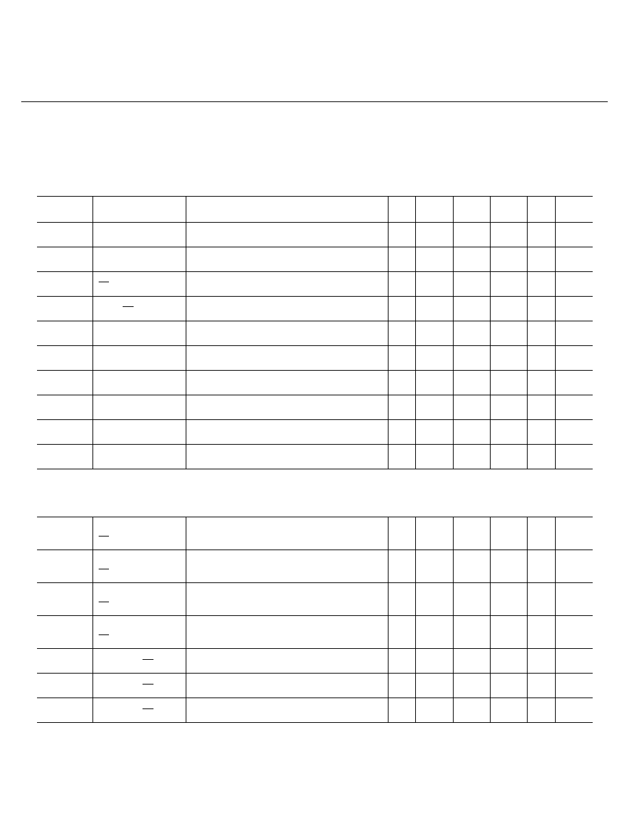
Electrical Characteristics
DC PARAMETER
(The following conditions apply to all the following parameters, unless otherwise specified.)
DC:
VCC 4.5V to 5.5V, Temp range: -55C to 125C
SYMBOL
PARAMETER
CONDITIONS
NOTES
PIN-
NAME
MIN
MAX
UNIT
SUB-
GROUPS
IIH
Input High
Current
VCC=5.5V, VM=2.7V, VINH=5.5V,
VINL=0.0V
1, 3 INPUTS
20
uA
1, 2,
3
IBVI
Input High
Current
VCC=5.5V, VM=7.0V, VINH=5.5V,
VINL=0.0V
1, 3 INPUTS
100
uA
1, 2,
3
IIL
Input LOW Current
MR, CP, CEP, Pn
VCC=5.5V, VM=0.5V, VINH=5.5V,
VINL=0.0V
1, 3 INPUTS
-0.6
mA
1, 2,
3
IIL2
Input LOW Current
CET, PE
VCC=5.5V, VM=0.5V, VINH=5.5V,
VINL=0.0V
1, 3 INPUTS
-1.2
mA
1, 2,
3
VOL
Output LOW
Voltage
VCC=4.5V, VIH=2.0V, IOL=20mA,
VINH=5.5V, VIL=0.8V, VINL=0.0V
1, 3 OUTPUTS
0.5
V
1, 2,
3
VOH
Output HIGH
Voltage
VCC=4.5V, VIL=0.8V, IOH=-1.0mA,
VIH=2.0V, VINH=5.5V, VINL=0.0V
1, 3 OUTPUTS 2.5
V
1, 2,
3
IOS
Short Circuit
Current
VCC=5.5V, VINH=5.5V, VM=0.0V,
VINL=0.0V
1, 3 OUTPUTS -60
-150
mA
1, 2,
3
VCD
Input Clamp Diode
Voltage
VCC=4.5V, IM=-18mA, VINH=5.5V
1, 3 INPUTS
-1.2
V
1, 2,
3
ICC
Supply Current
VCC=5.5V, VINL=0.0V, VINH=5.5V
1, 3 VCC
55
mA
1, 2,
3
ICEX
Output HIGH
Leakage Current
VCC=5.5V, VINL=0.0V, VINH=5.5V,
VM=5.5V
1, 3 OUTPUTS
250
uA
1, 2,
3
AC PARAMETER
(The following conditions apply to all the following parameters, unless otherwise specified.)
AC:
CL=50pf, RL=500 OHMS, TR=2.5ns, TF=2.5ns SEE AC FIGS
tpLH(1)
Propagation Delay
CP to Qn
PE=(High)
VCC=5.0V @25C, VCC=4.5V & 5.5V
@-55/125C
2, 4
3.5
7.5
ns
9
tpLH(1)
Propagation Delay
CP to Qn
PE=(High)
VCC=5.0V @25C, VCC=4.5V & 5.5V
@-55/125C
2, 4
3.5
9.0
ns
10, 11
tpHL(1)
Propagation Delay
CP to Qn
PE=(High)
VCC=5.0V @25C, VCC=4.5V & 5.5V
@-55/125C
2, 4
3.5
10.0
ns
9
tpHL(1)
Propagation Delay
CP to Qn
PE=(High)
VCC=5.0V @25C, VCC=4.5V & 5.5V
@-55/125C
2, 4
3.5
11.5
ns
10, 11
tpLH(2)
Propagation Delay
CP to Qn PE=(LOW)
VCC=5.0V @25C, VCC=4.5V & 5.5V
@-55/125C
2, 4
4.0
8.5
ns
9
tpLH(2)
Propagation Delay
CP to Qn PE=(LOW)
VCC=5.0V @25C, VCC=4.5V & 5.5V
@-55/125C
2, 4
4.0
10.0
ns
10, 11
tpHL(2)
Propagation Delay
CP to Qn PE=(LOW)
VCC=5.0V @25C, VCC=4.5V & 5.5V
@-55/125C
2, 4
4.0
8.5
ns
9
4

MN54F160A-X REV 1A0
MILITARY DATA SHEET
Electrical Characteristics
AC PARAMETER(Continued)
(The following conditions apply to all the following parameters, unless otherwise specified.)
AC:
CL=50pf, RL=500 OHMS, TR=2.5ns, TF=2.5ns SEE AC FIGS
SYMBOL
PARAMETER
CONDITIONS
NOTES
PIN-
NAME
MIN
MAX
UNIT
SUB-
GROUPS
tpHL(2)
Propagation Delay
CP to Qn PE=(LOW)
VCC=5.0V @25C, VCC=4.5V & 5.5V
@-55/125C
2, 4
4.0
10.0
ns
10, 11
tpLH(3)
Propagation Delay
VCC=5.0V @25C, VCC=4.5V & 5.5V
@-55/125C
2, 4 CP to
TC
5.0
14.0
ns
9
2, 4 CP to
TC
5.0
16.5
ns
10, 11
tpHL(3)
Propagation Delay
VCC=5.0V @25C, VCC=4.5V & 5.5V
@-55/125C
2, 4 CP to
TC
5.0
14.0
ns
9
2, 4 CP to
TC
5.0
15.5
ns
10, 11
tpLH(4)
Propagation Delay
VCC=5.0V @25C, VCC=4.5V & 5.5V
@-55/125C
2, 4 CET to
TC
2.5
7.5
ns
9
2, 4 CET to
TC
2.5
9.0
ns
10, 11
tpHL(4)
Propagation Delay
VCC=5.0V @25C, VCC=4.5V & 5.5V
@-55/125C
2, 4 CET to
TC
2.5
7.5
ns
9
2, 4 CET to
TC
2.5
9.0
ns
10, 11
tpHL(5)
Propagation Delay
VCC=5.0V @25C, VCC=4.5V & 5.5V
@-55/125C
2, 4 MR to
Qn
5.5
12.5
ns
9
2, 4 MR to
Qn
5.5
14.0
ns
10, 11
tpHL(6)
Propagation Delay
VCC=5.0V @25C, VCC=4.5V & 5.5V
@-55/125C
2, 4 MR to
TC
4.5
10.5
ns
9
2, 4 MR to
TC
4.5
12.5
ns
10, 11
ts(H/L)(1)
Setup Time (HIGH
or LOW)
VCC=5.0V @25C, VCC=4.5V & 5.5V
@-55/125C
5
Pn to
CP
5.0
ns
9
5
Pn to
CP
5.5
ns
10, 11
th(H/L)(1)
Hold Time (High
or Low)
VCC=5.0V @25C, VCC=4.5V & 5.5V
@-55/125C
5
Pn to
CP
2.0
ns
9
5
Pn to
CP
2.5
ns
10, 11
ts(H)(2)
Setup Time
(High)
VCC=5.0V @25C, VCC=4.5V & 5.5V
@-55/125C
5
PE to
CP
11.0
ns
9
5
PE to
CP
13.5
ns
10, 11
5
