
TL F 9494
54F74F190
UpDown
Decade
Counter
with
Preset
and
Ripple
Clock
November 1994
54F 74F190
Up Down Decade Counter with Preset and Ripple Clock
General Description
The 'F190 is a reversible BCD (8421) decade counter fea-
turing synchronous counting and asynchronous presetting
The preset feature allows the 'F190 to be used in program-
mable dividers The Count Enable input the Terminal Count
output and the Ripple Clock output make possible a variety
of methods of implementing multistage counters In the
counting modes state changes are initiated by the rising
edge of the clock
Features
Y
High-speed
125 MHz typical count frequency
Y
Synchronous counting
Y
Asynchronous parallel load
Y
Cascadable
Commercial
Military
Package
Package Description
Number
74F190PC
N16E
16-Lead (0 300 Wide) Molded Dual-In-Line
54F190DM (Note 2)
J16A
16-Lead Ceramic Dual-In-Line
74F190SC (Note 1)
M16A
16-Lead (0 150 Wide) Molded Small Outline JEDEC
54F190FM (Note 2)
W16A
16-Lead Cerpack
54F190LM (Note 2)
E20A
20-Lead Ceramic Leadless Chip Carrier Type C
Note 1
Devices also available in 13
reel Use suffix
e
SCX
Note 2
Military grade device with environmental and burn-in processing Use suffix
e
DMQB FMQB and LMQB
Logic Symbols
Connection Diagrams
TL F 9494 � 1
IEEE IEC
TL F 9494 � 4
Pin Assignment for
DIP SOIC and Flatpak
TL F 9494 � 2
Pin Assignment
for LCC
TL F 9494 � 3
TRI-STATE
is a registered trademark of National Semiconductor Corporation
C1995 National Semiconductor Corporation
RRD-B30M75 Printed in U S A
Unit Loading Fan Out
54F 74F
Pin Names
Description
U L
Input I
IH
I
IL
HIGH LOW
Output I
OH
I
OL
CE
Count Enable Input (Active LOW)
1 0 3 0
20 mA
b
1 8 mA
CP
Clock Pulse Input (Active Rising Edge)
1 0 1 0
20 mA
b
0 6 mA
P
0
� P
3
Parallel Data Inputs
1 0 1 0
20 mA
b
0 6 mA
PL
Asynchronous Parallel Load Input (Active LOW)
1 0 1 0
20 mA
b
0 6 mA
U D
Up Down Count Control Input
1 0 1 0
20 mA
b
0 6 mA
Q
0
� Q
3
Flip-Flop Outputs
50 33 3
b
1 mA 20 mA
RC
Ripple Clock Output (Active LOW)
50 33 3
b
1 mA 20 mA
TC
Terminal Count Output (Active HIGH)
50 33 3
b
1 mA 20 mA
Functional Description
The 'F190 is a synchronous up down BCD decade counter
containing four edge-triggered flip-flops with internal gating
and steering logic to provide individual preset count-up and
count-down operations It has an asynchronous parallel
load capability permitting the counter to be preset to any
desired number When the Parallel Load (PL) input is LOW
information present on the Parallel Data inputs (P
0
� P
3
) is
loaded into the counter and appears on the Q outputs This
operation overrides the counting functions as indicated in
the Mode Select Table A HIGH signal on the CE input inhib-
its counting When CE is LOW internal state changes are
initiated synchronously by the LOW-to-HIGH transition of
the clock input The direction of counting is determined by
the U D input signal as indicated in the Mode Select Table
CE and U D can be changed with the clock in either state
provided only that the recommended setup and hold times
are observed
Two types of outputs are provided as overflow underflow
indicators The Terminal Count (TC) output is normally LOW
and goes HIGH when a circuit reaches zero in the count-
down mode or reaches 9 in the count-up mode The TC
output will then remain HIGH until a state change occurs
whether by counting or presetting or until U D is changed
The TC output should not be used as a clock signal be-
cause it is subject to decoding spikes The TC signal is also
used internally to enable the Ripple Clock (RC) output The
RC output is normally HIGH When CE is LOW and TC is
HIGH the RC output will go LOW when the clock next goes
LOW and will stay LOW until the clock goes HIGH again
This feature simplifies the design of multistage counters
For a discussion and illustrations of the various methods of
implementing multistage counters please see the 'F191
data sheet
RC Truth Table
Inputs
Output
CE
TC
CP
RC
L
H
H
X
X
H
X
L
X
H
TC is generated internally
H
e
HIGH Voltage Level
L
e
LOW Voltage Level
X
e
Immaterial
L
e
LOW-to-HIGH Clock Transition
e
LOW Pulse
Mode Select Table
Inputs
Mode
PL
CE
U D
CP
H
L
L
L
Count Up
H
L
H
L
Count Down
L
X
X
X
Preset (Asyn )
H
H
X
X
No Change (Hold)
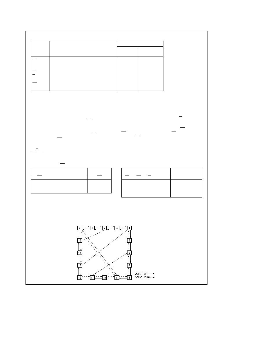
State Diagram
TL F 9494 � 5
2
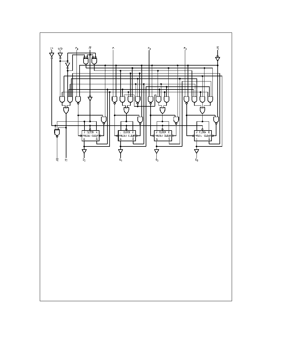
Logic Diagram
TL F 9494 � 6
Please note that this diagram is provided only for the understanding of logic operations and should not be used to estimate propagation delays
3

Absolute Maximum Ratings
(Note 1)
If Military Aerospace specified devices are required
please contact the National Semiconductor Sales
Office Distributors for availability and specifications
Storage Temperature
b
65 C to
a
150 C
Ambient Temperature under Bias
b
55 C to
a
125 C
Junction Temperature under Bias
b
55 C to
a
175 C
Plastic
b
55 C to
a
150 C
V
CC
Pin Potential to
Ground Pin
b
0 5V to
a
7 0V
Input Voltage (Note 2)
b
0 5V to
a
7 0V
Input Current (Note 2)
b
30 mA to
a
5 0 mA
Voltage Applied to Output
in HIGH State (with V
CC
e
0V)
Standard Output
b
0 5V to V
CC
TRI-STATE Output
b
0 5V to
a
5 5V
Current Applied to Output
in LOW State (Max)
twice the rated I
OL
(mA)
Note 1
Absolute maximum ratings are values beyond which the device may
be damaged or have its useful life impaired Functional operation under
these conditions is not implied
Note 2
Either voltage limit or current limit is sufficient to protect inputs
Recommended Operating
Conditions
Free Air Ambient Temperature
Military
b
55 C to
a
125 C
Commercial
0 C to
a
70 C
Supply Voltage
Military
a
4 5V to
a
5 5V
Commercial
a
4 5V to
a
5 5V
DC Electrical Characteristics
Symbol
Parameter
54F 74F
Units
V
CC
Conditions
Min
Typ
Max
V
IH
Input HIGH Voltage
2 0
V
Recognized as a HIGH Signal
V
IL
Input LOW Voltage
0 8
V
Recognized as a LOW Signal
V
CD
Input Clamp Diode Voltage
b
1 2
V
Min
I
IN
e b
18 mA
V
OH
Output HIGH
54F 10% V
CC
2 5
I
OH
e b
1 mA
Voltage
74F 10% V
CC
2 5
V
Min
I
OH
e b
1 mA
74F 5% V
CC
2 7
I
OH
e b
1 mA
V
OL
Output LOW
54F 10% V
CC
0 5
V
Min
I
OL
e
20 mA
Voltage
74F 10% V
CC
0 5
I
OL
e
20 mA
I
IH
Input HIGH
54F
20 0
m
A
Max
V
IN
e
2 7V
Current
74F
5 0
I
BVI
Input HIGH Current
54F
100
m
A
Max
V
IN
e
7 0V
Breakdown Test
74F
7 0
I
CEX
Output HIGH
54F
250
m
A
Max
V
OUT
e
V
CC
Leakage Current
74F
50
V
ID
Input Leakage
74F
4 75
V
0 0
I
ID
e
1 9 mA
Test
All Other Pins Grounded
I
OD
Output Leakage
74F
3 75
m
A
0 0
V
IOD
e
150 mV
Circuit Current
All Other Pins Grounded
I
IL
Input LOW Current
b
0 6
mA
Max
V
IN
e
0 5V except CE
b
1 8
V
IN
e
0 5V CE
I
OS
Output Short-Circuit Current
b
60
b
150
mA
Max
V
OUT
e
0V
I
CCL
Power Supply Current
38
55
mA
Max
V
O
e
LOW
4

AC Electrical Characteristics
74F
54F
74F
T
A
e a
25 C
T
A
V
CC
e
Mil
T
A
V
CC
e
Com
Symbol
Parameter
V
CC
e a
5 0V
C
L
e
50 pF
C
L
e
50 pF
Units
C
L
e
50 pF
Min
Typ
Max
Min
Max
Min
Max
f
max
Maximum Clock Frequency
100
125
75
90
MHz
t
PLH
Propagation Delay
3 0
5 5
7 5
3 0
9 5
3 0
8 5
t
PHL
CP to Q
n
5 0
8 5
11 0
5 0
13 5
5 0
12 0
ns
t
PLH
Propagation Delay
6 0
10 0
13 0
6 0
16 5
6 0
14 0
t
PHL
CP to TC
5 0
8 5
11 0
5 0
13 5
5 0
12 0
t
PLH
Propagation Delay
3 0
5 5
7 5
3 0
9 5
3 0
8 5
t
PHL
CP to RC
3 0
5 0
7 0
3 0
9 0
3 0
8 0
ns
t
PLH
Propagation Delay
3 0
5 0
7 0
3 0
9 0
3 0
8 0
t
PHL
CE to RC
3 0
5 5
7 0
3 0
9 0
3 0
8 0
t
PLH
Propagation Delay
7 0
11 0
18 0
7 0
22 0
7 0
20 0
t
PHL
U D to RC
5 5
9 0
12 0
5 5
14 0
5 5
13 0
ns
t
PLH
Propagation Delay
4 0
7 0
10 0
4 0
13 5
4 0
11 0
t
PHL
U D to TC
4 0
6 5
10 0
4 0
12 5
4 0
11 0
t
PLH
Propagation Delay
3 0
4 5
7 0
3 0
9 0
3 0
8 0
ns
t
PHL
P
n
to Q
n
6 0
10 0
13 0
6 0
16 0
6 0
14 0
t
PLH
Propagation Delay
5 0
8 5
11 0
5 0
13 0
5 0
12 0
ns
t
PHL
PL to Q
n
5 5
9 0
12 0
5 5
14 5
5 5
13 0
AC Operating Requirements
74F
54F
74F
Symbol
Parameter
T
A
e a
25 C
T
A
V
CC
e
Mil
T
A
V
CC
e
Com
Units
V
CC
e a
5 0V
Min
Max
Min
Max
Min
Max
t
s
(H)
Setup Time HIGH or LOW
4 5
6 0
5 0
t
s
(L)
P
n
to PL
4 5
6 0
5 0
ns
t
h
(H)
Hold Time HIGH or LOW
2 0
2 0
2 0
t
h
(L)
P
n
to PL
2 0
2 0
2 0
t
s
(L)
Setup Time LOW
10 0
10 5
10 0
CE to CP
ns
t
h
(L)
Hold Time LOW
0
0
0
CE to CP
t
s
(H)
Setup Time HIGH or LOW
12 0
12 0
12 0
t
s
(L)
U D to CP
12 0
12 0
12 0
ns
t
h
(H)
Hold Time HIGH or LOW
0
0
0
t
h
(L)
U D to CP
0
0
0
t
w
(L)
PL Pulse Width LOW
6 0
8 5
6 0
ns
t
w
(L)
CP Pulse Width LOW
5 0
7 0
5 0
ns
t
rec
Recovery Time PL to CP
6 0
7 5
6 0
ns
5
Ordering Information
The device number is used to form part of a simplified purchasing code where the package type and temperature range are
defined as follows
74F
190
S
C
X
Temperature Range Family
Special Variations
74F
e
Commercial
X
e
Devices shipped in 13 reels
54F
e
Military
QB
e
Military grade device with
environmental and burn-in
Device Type
processing shipped in tubes
Package Code
Temperature Range
P
e
Plastic DIP
C
e
Commercial (0 C to
a
70 C)
D
e
Ceramic DIP
M
e
Military (
b
55 C to
a
125 C)
F
e
Flatpak
L
e
Leadless Chip Carrier (LCC)
S
e
Small Outline SOIC JEDEC
6

7
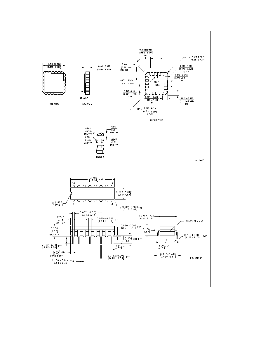
Physical Dimensions
inches (millimeters)
20-Lead Ceramic Leadless Chip Carrier (L)
NS Package Number E20A
16-Lead Ceramic Dual-In-Line Package (D)
NS Package Number J16A
8
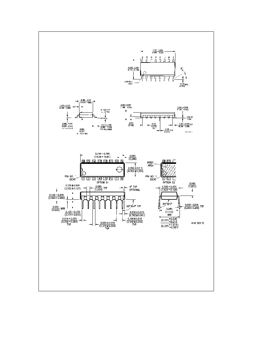
Physical Dimensions
inches (millimeters) (Continued)
16-Lead (0 150 Wide) Molded Small Outline Package JEDEC (S)
NS Package Number M16A
16-Lead (0 300 Wide) Molded Dual-In-Line Package (P)
NS Package Number N16E
9
54F74F190
UpDown
Decade
Counter
with
Preset
and
Ripple
Clock
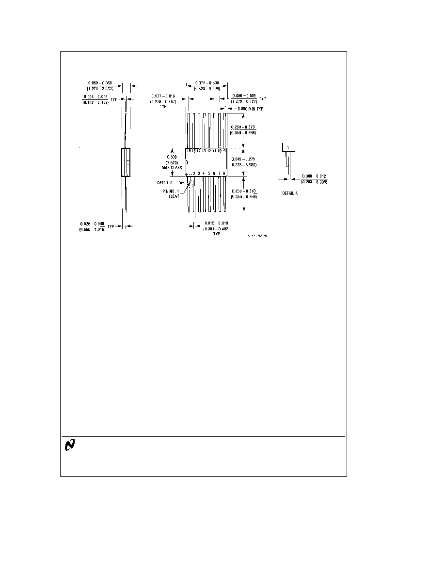
Physical Dimensions
inches (millimeters) (Continued)
16-Lead Ceramic Flatpak (F)
NS Package Number W16A
LIFE SUPPORT POLICY
NATIONAL'S PRODUCTS ARE NOT AUTHORIZED FOR USE AS CRITICAL COMPONENTS IN LIFE SUPPORT
DEVICES OR SYSTEMS WITHOUT THE EXPRESS WRITTEN APPROVAL OF THE PRESIDENT OF NATIONAL
SEMICONDUCTOR CORPORATION As used herein
1 Life support devices or systems are devices or
2 A critical component is any component of a life
systems which (a) are intended for surgical implant
support device or system whose failure to perform can
into the body or (b) support or sustain life and whose
be reasonably expected to cause the failure of the life
failure to perform when properly used in accordance
support device or system or to affect its safety or
with instructions for use provided in the labeling can
effectiveness
be reasonably expected to result in a significant injury
to the user
National Semiconductor
National Semiconductor
National Semiconductor
National Semiconductor
National Semiconductores
National Semiconductor
Corporation
GmbH
Japan Ltd
Hong Kong Ltd
Do Brazil Ltda
(Australia) Pty Ltd
2900 Semiconductor Drive
Livry-Gargan-Str 10
Sumitomo Chemical
13th Floor Straight Block
Rue Deputado Lacorda Franco
Building 16
P O Box 58090
D-82256 F4urstenfeldbruck
Engineering Center
Ocean Centre 5 Canton Rd
120-3A
Business Park Drive
Santa Clara CA 95052-8090
Germany
Bldg 7F
Tsimshatsui Kowloon
Sao Paulo-SP
Monash Business Park
Tel 1(800) 272-9959
Tel (81-41) 35-0
1-7-1 Nakase Mihama-Ku
Hong Kong
Brazil 05418-000
Nottinghill Melbourne
TWX (910) 339-9240
Telex 527649
Chiba-City
Tel (852) 2737-1600
Tel (55-11) 212-5066
Victoria 3168 Australia
Fax (81-41) 35-1
Ciba Prefecture 261
Fax (852) 2736-9960
Telex 391-1131931 NSBR BR
Tel (3) 558-9999
Tel (043) 299-2300
Fax (55-11) 212-1181
Fax (3) 558-9998
Fax (043) 299-2500
National does not assume any responsibility for use of any circuitry described no circuit patent licenses are implied and National reserves the right at any time without notice to change said circuitry and specifications