TL F 9497
54F74F193
UpDown
Binary
Counter
with
Separate
UpDown
Clocks
November 1994
54F 74F193 Up Down Binary Counter
with Separate Up Down Clocks
General Description
The 'F193 is an up down modulo-16 binary counter Sepa-
rate Count Up and Count Down Clocks are used and in
either counting mode the circuits operate synchronously
The outputs change state synchronously with the LOW-to-
HIGH transitions on the clock inputs Separate Terminal
Count Up and Terminal Count Down outputs are provided
that are used as the clocks for subsequent stages without
extra logic thus simplifying multi-stage counter designs
Individual preset inputs allow the circuit to be used as a
programmable counter Both the Parallel Load (PL) and the
Master Reset (MR) inputs asynchronously override the
clocks
Features
Y
Guaranteed 4000V minimum ESD protection
Commercial
Military
Package
Package Description
Number
74F193PC
N16E
16-Lead (0 300 Wide) Molded Dual-In-Line
54F193DM (Note 2)
J16A
16-Lead Ceramic Dual-In-Line
74F193SC (Note 1)
M16A
16-Lead (0 150 Wide) Molded Small Outline JEDEC
74F193SJ (Note 1)
M16D
16-Lead (0 300 Wide) Molded Small Outline EIAJ
54F193FM (Note 2)
W16A
16-Lead Cerpack
54F193LM (Note 2)
E20A
20-Lead Ceramic Leadless Chip Carrier Type C
Note 1
Devices also available in 13
reel Use suffix
e
SCX and SJX
Note 2
Military grade device with environmental and burn-in processing Use suffix
e
DMQB FMQB and LMQB
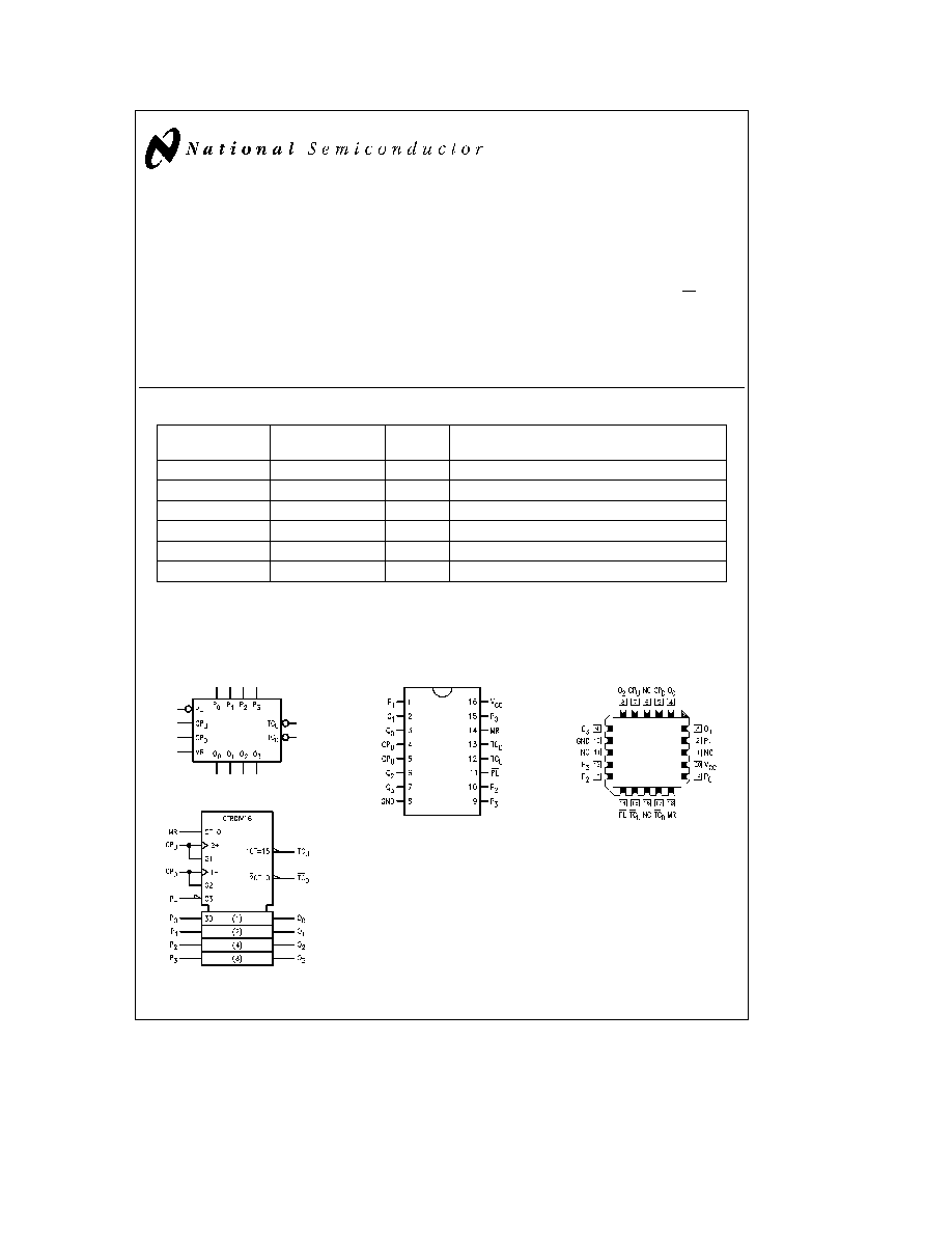
Logic Symbols
Connection Diagrams
TL F 9497 � 1
IEEE IEC
TL F 9497 � 4
Pin Assignment
for DIP SOIC and Flatpak
TL F 9497 � 2
Pin Assignment
for LCC
TL F 9497 � 3
TRI-STATE
is a registered trademark of National Semiconductor Corporation
C1995 National Semiconductor Corporation
RRD-B30M75 Printed in U S A
Unit Loading Fan Out
54F 74F
Pin Names
Description
U L
Input I
IH
I
IL
HIGH LOW Output I
OH
I
OL
CP
U
Count Up Clock Input (Active Rising Edge)
1 0 3 0
20 mA
b
1 8 mA
CP
D
Count Down Clock Input (Active Rising Edge)
1 0 3 0
20 mA
b
1 8 mA
MR
Asynchronous Master Reset Input (Active HIGH)
1 0 1 0
20 mA
b
0 6 mA
PL
Asynchronous Parallel Load Input (Active LOW)
1 0 1 0
20 mA
b
0 6 mA
P
0
� P
3
Parallel Data Inputs
1 0 1 0
20 mA
b
0 6 mA
Q
0
� Q
3
Flip-Flop Outputs
50 33 3
b
1 mA 20 mA
TC
D
Terminal Count Down (Borrow) Output (Active LOW)
50 33 3
b
1 mA 20 mA
TC
U
Terminal Count Up (Carry) Output (Active LOW)
50 33 3
b
1 mA 20 mA
Functional Description
The 'F193 is a 4-bit binary synchronous up down (revers-
ible) counter It contains four edge-triggered flip-flops with
internal gating and steering logic to provide master reset
individual preset count up and count down operations
A LOW-to-HIGH transition on the CP input to each flip-flop
causes the output to change state Synchronous switching
as opposed to ripple counting is achieved by driving the
steering gates of all stages from a common Count Up line
and a common Count Down line thereby causing all state
changes to be initiated simultaneously A LOW-to-HIGH
transition on the Count Up input will advance the count by
one a similar transition on the Count Down input will de-
crease the count by one While counting with one clock in-
put the other should be held HIGH as indicated in the
Function Table
The Terminal Count Up (TC
U
) and Terminal Count Down
(TC
D
) outputs are normally HIGH When the circuit has
reached the maximum count state 15 the next HIGH-to-
LOW transition of the Count Up Clock will cause TC
U
to go
LOW TC
U
will stay LOW until CP
U
goes HIGH again thus
effectively repeating the Count Up Clock but delayed by
two gate delays Similarly the TC
D
output will go LOW when
the circuit is in the zero state and the Count Down Clock
goes LOW Since the TC outputs repeat the clock wave-
forms they can be used as the clock input signals to the
next higher order circuit in a multistage counter
TC
U
e
Q
0
Q
1
Q
2
Q
3
CP
U
TC
D
e
Q
0
Q
1
Q
2
Q
3
CP
D
The 'F193 has an asynchronous parallel load capability per-
mitting the counter to be preset When the Parallel Load
(PL) and the Master Reset (MR) inputs are LOW informa-
tion present on the Parallel Data input (P
0
� P
3
) is loaded
into the counter and appears on the outputs regardless of
the conditions of the clock inputs A HIGH signal on the
Master Reset input will disable the preset gates override
both clock inputs and latch each Q output in the LOW state
If one of the clock inputs is LOW during and after a reset or
load operation the next LOW-to-HIGH transition of that
clock will be interpreted as a legitimate signal and will be
counted
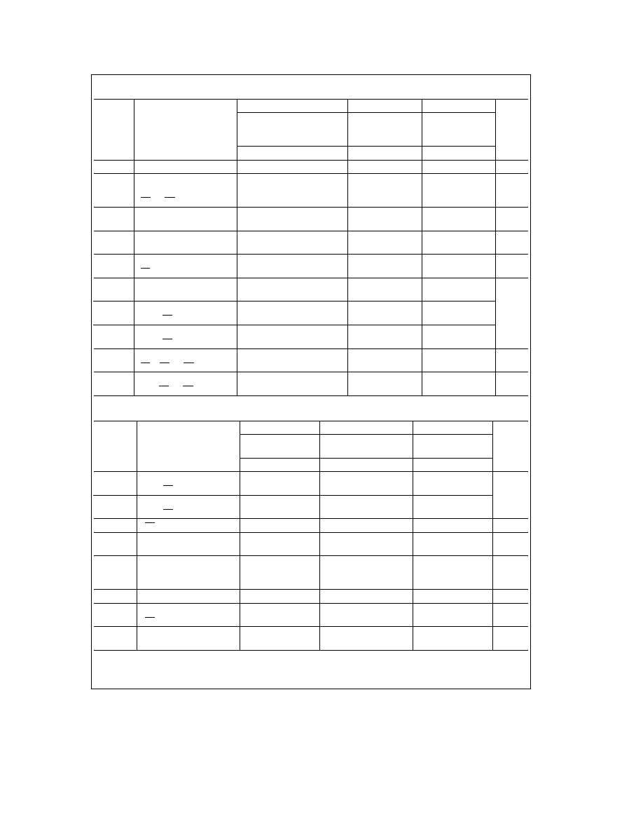
Function Table
MR
PL
CP
U
CP
D
Mode
H
X
X
X
Reset (Asyn )
L
L
X
X
Preset (Asyn )
L
H
H
H
No Change
L
H
L
H
Count Up
L
H
H
L
Count Down
H
e
HIGH Voltage Level
L
e
LOW Voltage Level
X
e
Immaterial
L
e
LOW-to-HIGH Clock Transition
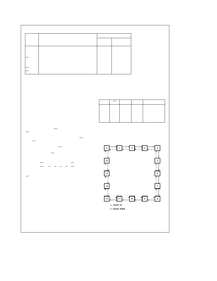
State Diagram
TL F 9497 � 5
2
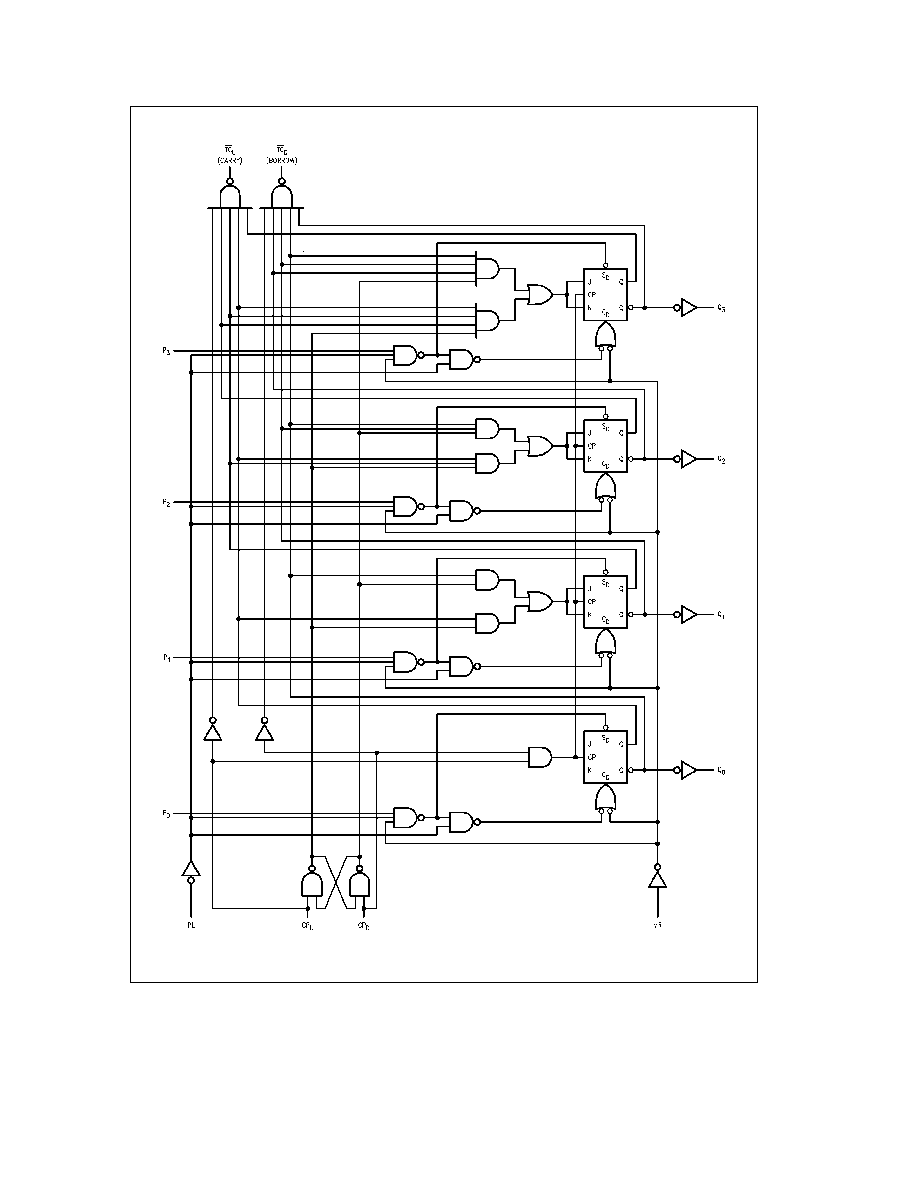
Logic Diagram
TL F 9497 � 6
Please note that this diagram is provided only for the understanding of logic operations and should not be used to estimate propagation delays
3

Absolute Maximum Ratings
(Note 1)
If Military Aerospace specified devices are required
please contact the National Semiconductor Sales
Office Distributors for availability and specifications
Storage Temperature
b
65 C to
a
150 C
Ambient Temperature under Bias
b
55 C to
a
125 C
Junction Temperature under Bias
b
55 C to
a
175 C
Plastic
b
55 C to
a
150 C
V
CC
Pin Potential to
Ground Pin
b
0 5V to
a
7 0V
Input Voltage (Note 2)
b
0 5V to
a
7 0V
Input Current (Note 2)
b
30 mA to
a
5 0 mA
Voltage Applied to Output
in HIGH State (with V
CC
e
0V)
Standard Output
b
0 5V to V
CC
TRI-STATE Output
b
0 5V to
a
5 5V
Current Applied to Output
in LOW State (Max)
twice the rated I
OL
(mA)
ESD Last Passing Voltage (Min)
4000V
Note 1
Absolute maximum ratings are values beyond which the device may
be damaged or have its useful life impaired Functional operation under
these conditions is not implied
Note 2
Either voltage limit or current limit is sufficient to protect inputs
Recommended Operating
Conditions
Free Air Ambient Temperature
Military
b
55 C to
a
125 C
Commercial
0 C to
a
70 C
Supply Voltage
Military
a
4 5V to
a
5 5V
Commercial
a
4 5V to
a
5 5V
DC Electrical Characteristics
Symbol
Parameter
54F 74F
Units
V
CC
Conditions
Min
Typ
Max
V
IH
Input HIGH Voltage
2 0
V
Recognized as a HIGH Signal
V
IL
Input LOW Voltage
0 8
V
Recognized as a LOW Signal
V
CD
Input Clamp Diode Voltage
b
1 2
V
Min
I
IN
e b
18 mA
V
OH
Output HIGH
54F 10% V
CC
2 5
I
OH
e b
1 mA
Voltage
74F 10% V
CC
2 5
V
Min
I
OH
e b
1 mA
74F 5% V
CC
2 7
I
OH
e b
1 mA
V
OL
Output LOW
54F 10% V
CC
0 5
V
Min
I
OL
e
20 mA
Voltage
74F 10% V
CC
0 5
I
OL
e
20 mA
I
IH
Input HIGH
54F
20 0
m
A
Max
V
IN
e
2 7V
Current
74F
5 0
I
BVI
Input HIGH Current
54F
100
m
A
Max
V
IN
e
7 0V
Breakdown Test
74F
7 0
I
CEX
Output HIGH
54F
250
m
A
Max
V
OUT
e
V
CC
Leakage Current
74F
50
V
ID
Input Leakage
74F
4 75
V
0 0
I
ID
e
1 9 mA
Test
All Other Pins Grounded
I
OD
Output Leakage
74F
3 75
m
A
0 0
V
IOD
e
150 mV
Circuit Current
All Other Pins Grounded
I
IL
Input LOW Current
b
0 6
mA
Max
V
IN
e
0 5V (MR PL P
n
)
b
1 8
V
IN
e
0 5V (CP
u
CP
D
)
I
OS
Output Short-Circuit Current
b
60
b
150
mA
Max
V
OUT
e
0V
I
CC
Power Supply Current
38
55
mA
Max
4
AC Electrical Characteristics
74F
54F
74F
T
A
e a
25 C
T
A
V
CC
e
Mil
T
A
V
CC
e
Com
Symbol
Parameter
V
CC
e a
5 0V
C
L
e
50 pF
C
L
e
50 pF
Units
C
L
e
50 pF
Min
Typ
Max
Min
Max
Min
Max
f
max
Maximum Count Frequency
100
125
75
90
MHz
t
PLH
Propagation Delay
4 0
7 0
9 0
4 0
10 5
4 0
10 0
t
PHL
CP
U
or CP
D
to
3 5
6 0
8 0
3 5
9 5
3 5
9 0
ns
TC
U
or TC
D
t
PLH
Propagation Delay
4 0
6 5
8 5
3 5
10 0
4 0
9 5
ns
t
PHL
CP
U
or CP
D
to Q
n
5 5
9 5
12 5
5 5
14 0
5 5
13 5
t
PLH
Propagation Delay
3 0
4 5
7 0
3 0
8 5
3 0
8 0
ns
t
PHL
P
n
to Q
n
6 0
11 0
14 5
6 0
16 5
6 0
15 5
t
PLH
Propagation Delay
5 0
8 5
11 0
5 0
13 5
5 0
12 0
ns
t
PHL
PL to Q
n
5 5
10 0
13 0
5 5
15 0
5 5
14 0
t
PHL
Propagation Delay
5 5
11 0
14 5
5 0
16 0
5 5
15 5
MR to Q
n
t
PLH
Propagation Delay
6 0
10 5
13 5
5 0
15 0
6 0
14 5
ns
MR to TC
U
t
PHL
Propagation Delay
6 0
11 5
14 5
6 0
16 0
6 0
15 5
MR to TC
D
t
PLH
Propagation Delay
7 0
12 0
15 5
7 0
18 5
7 0
16 5
ns
t
PHL
PL to TC
U
or TC
D
7 0
11 5
14 5
6 0
17 5
7 0
15 5
t
PLH
Propagation Delay
7 0
11 5
14 5
6 0
16 5
7 0
15 5
ns
t
PHL
P
n
to TC
U
or TC
D
6 5
11 0
14 0
5 0
16 5
6 5
15 0
AC Operating Requirements
74F
54F
74F
Symbol
Parameter
T
A
e a
25 C
T
A
V
CC
e
Mil
T
A
V
CC
e
Com
Units
V
CC
e a
5 0V
Min
Max
Min
Max
Min
Max
t
s
(H)
Setup Time HIGH or LOW
4 5
6 0
5 0
t
s
(L)
P
n
to PL
4 5
6 0
5 0
t
h
(H)
Hold Time HIGH or LOW
2 0
2 0
2 0
ns
t
h
(L)
P
n
to PL
2 0
2 0
2 0
t
w
(L)
PL Pulse Width LOW
6 0
7 5
6 0
ns
t
w
(L)
CP
U
or CP
D
5 0
7 0
5 0
ns
Pulse Width LOW
t
w
(L)
CP
U
or CP
D
Pulse Width LOW
10 0
12 0
10 0
ns
(Change of Direction)
t
w
(H)
MR Pulse Width HIGH
6 0
6 0
6 0
ns
t
rec
Recovery Time
6 0
8 0
6 0
ns
PL to CP
U
or CP
D
t
rec
Recovery Time
4 0
4 5
4 0
ns
MR to CP
U
or CP
D
5