 | –≠–ª–µ–∫—Ç—Ä–æ–Ω–Ω—ã–π –∫–æ–º–ø–æ–Ω–µ–Ω—Ç: 54F283DM | –°–∫–∞—á–∞—Ç—å:  PDF PDF  ZIP ZIP |

TL F 9513
54F74F283
4-Bit
Binary
Full
Adder
with
Fast
Carry
November 1994
54F 74F283
4-Bit Binary Full Adder with Fast Carry
General Description
The 'F283 high-speed 4-bit binary full adder with internal
carry lookahead accepts two 4-bit binary words (A
0
≠ A
3
B
0
≠ B
3
) and a Carry input (C
0
) It generates the binary Sum
outputs (S
0
≠ S
3
) and the Carry output (C
4
) from the most
significant bit The 'F283 will operate with either active
HIGH or active LOW operands (positive or negative logic)
Features
Y
Guaranteed 4000V minimum ESD protection
Commercial
Military
Package
Package Description
Number
74F283PC
N16E
16-Lead (0 300 Wide) Molded Dual-In-Line
54F283DM (Note 2)
J16A
16-Lead Ceramic Dual-In-Line
74F283SC (Note 1)
M16A
16-Lead (0 150 Wide) Molded Small Outline JEDEC
74F283SJ (Note 1)
M16D
16-Lead (0 300 Wide) Molded Small Outline EIAJ
54F283FM (Note 2)
W16A
16-Lead Cerpack
54F283LL (Note 2)
E20A
20-Lead Ceramic Leadless Chip Carrier Type C
Note 1
Devices also available in 13
reel Use suffix
e
SCX and SJX
Note 2
Military grade device with environmental and burn-in processing Use suffix
e
DMQB FMQB and LMQB
Logic Symbols
Connection Diagrams
TL F 9513 ≠ 1
IEEE IEC
TL F 9513 ≠ 4
Pin Assignment
for DIP SOIC and Flatpak
TL F 9513 ≠ 2
Pin Assignment
for LCC
TL F 9513 ≠ 3
TRI-STATE
is a registered trademark of National Semiconductor Corporation
C1995 National Semiconductor Corporation
RRD-B30M105 Printed in U S A
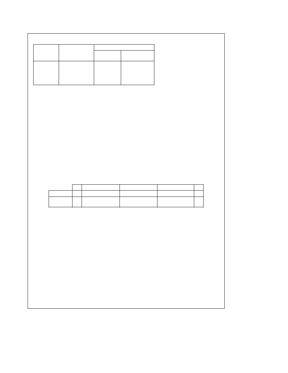
Unit Loading Fan Out
54F 74F
Pin Names
Description
U L
Input I
IH
I
IL
HIGH LOW
Output I
OH
I
OL
A
0
≠ A
3
A Operand Inputs
1 0 2 0
20 mA
b
1 2 mA
B
0
≠ B
3
B Operand Inputs
1 0 2 0
20 mA
b
1 2 mA
C
0
Carry Input
1 0 1 0
20 mA
b
0 6 mA
S
0
≠ S
3
Sum Outputs
50 33 3
b
1 mA 20 mA
C
4
Carry Output
50 33 3
b
1 mA 20 mA
Functional Description
The 'F283 adds two 4-bit binary words (A plus B) plus the
incoming Carry (C
0
) The binary sum appears on the Sum
(S
0
≠ S
3
) and outgoing carry (C
4
) outputs The binary weight
of the various inputs and outputs is indicated by the sub-
script numbers representing powers of two
2
0
(A
0
a
B
0
a
C
0
)
a
2
1
(A
1
a
B
1
)
a
2
2
(A
2
a
B
2
)
a
2
3
(A
3
a
B
3
)
e
S
0
a
2S
1
a
4S
2
a
8S
3
a
16C
4
Where (
a
)
e
plus
Interchanging inputs of equal weight does not affect the op-
eration Thus C
0
A
0
B
0
can be arbitrarily assigned to pins
5 6 and 7 for DIPS and 7 8 and 9 for chip carrier packages
Due to the symmetry of the binary add function the 'F283
can be used either with all inputs and outputs active HIGH
(positive logic) or with all inputs and outputs active LOW
(negative logic) See
Figure 1 Note that if C
0
is not used it
must be tied LOW for active HIGH logic or tied HIGH for
active LOW logic
Due to pin limitations the intermediate carries of the 'F283
are not brought out for use as inputs or outputs However
other means can be used to effectively insert a carry into or
bring a carry out from an intermediate stage
Figure 2
shows how to make a 3-bit adder Tying the operand inputs
of the fourth adder (A
3
B
3
) LOW makes S
3
dependent only
on and equal to the carry from the third adder Using some-
what the same principle
Figure 3 shows a way of dividing
the 'F283 into a 2-bit and a 1-bit adder The third stage
adder (A
2
B
2
S
2
) is used merely as a means of getting a
carry (C
10
) signal into the fourth stage (via A
2
and B
2
) and
bringing out the carry from the second stage on S
2
Note
that as long as A
2
and B
2
are the same whether HIGH or
LOW they do not influence S
2
Similarly when A
2
and B
2
are the same the carry into the third stage does not influ-
ence the carry out of the third stage
Figure 4 shows a meth-
od of implementing a 5-input encoder where the inputs are
equally weighted The outputs S
0
S
1
and S
2
present a bina-
ry number equal to the number of inputs I
1
≠ I
5
that are true
Figure 5 shows one method of implementing a 5-input ma-
jority gate When three or more of the inputs I
1
≠ I
5
are true
the output M
5
is true
C
0
A
0
A
1
A
2
A
3
B
0
B
1
B
2
B
3
S
0
S
1
S
2
S
3
C
4
Logic Levels
L
L
H
L
H
H
L
L
H
H
H
L
L
H
Active HIGH
0
0
1
0
1
1
0
0
1
1
1
0
0
1
Active LOW
1
1
0
1
0
0
1
1
0
0
0
1
1
0
Active HIGH 0
a
10
a
9
e
3
a
16
Active LOW 1
a
5
a
6
e
12
a
0
FIGURE 1 Active HIGH versus Active LOW Interpretation
2

Functional Description
(Continued)
TL F 9513 ≠ 5
FIGURE 2 3-Bit Adder
TL F 9513 ≠ 6
FIGURE 3 2-Bit and 1-Bit Adders
TL F 9513 ≠ 7
FIGURE 4 5-Input Encoder
TL F 9513 ≠ 8
FIGURE 5 5-Input Majority Gate
3

Logic Diagram
TLF9513
≠
9
Please note that this diagram is provided only for the understanding of logic operations and should not be used to estimate propagation delays
4

Absolute Maximum Ratings
(Note 1)
If Military Aerospace specified devices are required
please contact the National Semiconductor Sales
Office Distributors for availability and specifications
Storage Temperature
b
65 C to
a
150 C
Ambient Temperature under Bias
b
55 C to
a
125 C
Junction Temperature under Bias
b
55 C to
a
175 C
Plastic
b
55 C to
a
150 C
V
CC
Pin Potential to
Ground Pin
b
0 5V to
a
7 0V
Input Voltage (Note 2)
b
0 5V to
a
7 0V
Input Current (Note 2)
b
30 mA to
a
5 0 mA
Voltage Applied to Output
in HIGH State (with V
CC
e
0V)
Standard Output
b
0 5V to V
CC
TRI-STATE Output
b
0 5V to
a
5 5V
Current Applied to Output
in LOW State (Max)
twice the rated I
OL
(mA)
ESD Last Passing Voltage (Min)
4000V
Note 1
Absolute maximum ratings are values beyond which the device may
be damaged or have its useful life impaired Functional operation under
these conditions is not implied
Note 2
Either voltage limit or current limit is sufficient to protect inputs
Recommended Operating
Conditions
Free Air Ambient Temperature
Military
b
55 C to
a
125 C
Commercial
0 C to
a
70 C
Supply Voltage
Military
a
4 5V to
a
5 5V
Commercial
a
4 5V to
a
5 5V
DC Electrical Characteristics
Symbol
Parameter
54F 74F
Units
V
CC
Conditions
Min
Typ
Max
V
IH
Input HIGH Voltage
2 0
V
Recognized as a HIGH Signal
V
IL
Input LOW Voltage
0 8
V
Recognized as a LOW Signal
V
CD
Input Clamp Diode Voltage
b
1 2
V
Min
I
IN
e b
18 mA
V
OH
Output HIGH
54F 10% V
CC
2 5
I
OH
e b
1 mA
Voltage
74F 10% V
CC
2 5
V
Min
I
OH
e b
1 mA
74F 5% V
CC
2 7
I
OH
e b
1 mA
V
OL
Output LOW
54F 10% V
CC
0 5
V
Min
I
OL
e
20 mA
Voltage
74F 10% V
CC
0 5
I
OL
e
20 mA
I
IH
Input HIGH Current
54F
20 0
m
A
Max
V
IN
e
2 7V
74F
5 0
I
BVI
Input HIGH Current
54F
100
m
A
Max
V
IN
e
7 0V
Breakdown Test
74F
7 0
I
CEX
Output HIGH
54F
250
m
A
Max
V
OUT
e
V
CC
Leakage Current
74F
50
V
ID
Input Leakage Test
74F
4 75
V
0 0
I
ID
e
1 9 mA
All Other Pins Grounded
I
OD
Output Leakage
74F
3 75
m
A
0 0
V
IOD
e
150 mV
Circuit Current
All Other Pins Grounded
I
IL
Input LOW Current
b
0 6
mA
Max
V
IN
e
0 5V (C
O
)
b
1 2
V
IN
e
0 5V (A
n
B
n
)
I
OS
Output Short-Circuit Current
b
60
b
150
mA
Max
V
OUT
e
0V
I
CCH
Power Supply Current
36
55
mA
Max
V
O
e
HIGH
I
CCL
Power Supply Current
36
55
mA
Max
V
O
e
LOW
5

AC Electrical Characteristics
74F
54F
74F
T
A
e a
25 C
T
A
V
CC
e
Mil
T
A
V
CC
e
Com
Symbol
Parameter
V
CC
e a
5 0V
C
L
e
50 pF
C
L
e
50 pF
Units
C
L
e
50 pF
Min
Typ
Max
Min
Max
Min
Max
t
PLH
Propagation Delay
3 5
7 0
9 5
3 5
14 0
3 5
11 0
ns
t
PHL
C
0
to S
n
3 0
7 0
9 5
3 0
14 0
3 0
11 0
t
PLH
Propagation Delay
3 0
7 0
9 5
3 0
17 0
3 0
13 0
ns
t
PHL
A
n
or B
n
to S
n
3 0
7 0
9 5
3 0
14 0
3 0
11 5
t
PLH
Propagation Delay
3 0
5 7
7 5
3 0
10 5
3 0
8 5
ns
t
PHL
C
0
to C
4
3 0
5 4
7 0
2 5
10 0
3 0
8 0
t
PLH
Propagation Delay
3 0
5 7
7 5
3 0
10 5
3 0
8 5
ns
t
PHL
A
n
or B
n
to C
4
2 5
5 3
7 0
2 5
10 0
2 5
8 0
Ordering Information
The device number is used to form part of a simplified purchasing code where the package type and temperature range are
defined as follows
74F
283
S
C
X
Temperature Range Family
Special Variations
74F
e
Commercial
QB
e
Military grade device with
54F
e
Military
environmental and burn-in
processing
Device Type
X
e
Devices shipped in 13 reel
Package Code
Temperature Range
P
e
Plastic DIP
C
e
Commercial (0 C to
a
70 C)
D
e
Ceramic DIP
M
e
Military (
b
55 C to
a
125 C)
F
e
Flatpak
L
e
Leadless Chip Carrier (LCC)
S
e
Small Outline SOIC JEDEC
SJ
e
Small Outline SOIC EIAJ
6

Physical Dimensions
inches (millimeters)
20-Lead Ceramic Leadless Chip Carrier (L)
NS Package Number E20A
16-Lead Ceramic Dual-In-Line Package (D)
NS Package Number J16A
7

Physical Dimensions
inches (millimeters) (Continued)
16-Lead (0 150 Wide) Molded Small Outline Package JEDEC (S)
NS Package Number M16A
16-Lead (0 300 Wide) Molded Small Outline Package EIAJ (SJ)
NS Package Number M16D
8
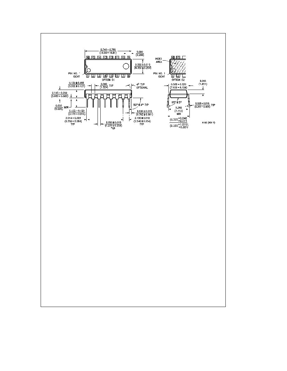
Physical Dimensions
inches (millimeters) (Continued)
16-Lead (0 300 Wide) Molded Dual-In-Line Package (P)
NS Package Number N16E
9

54F74F283
4-Bit
Binary
Full
Adder
with
Fast
Carry
Physical Dimensions
inches (millimeters) (Continued)
16-Lead Ceramic Flatpak (F)
NS Package Number W16A
LIFE SUPPORT POLICY
NATIONAL'S PRODUCTS ARE NOT AUTHORIZED FOR USE AS CRITICAL COMPONENTS IN LIFE SUPPORT
DEVICES OR SYSTEMS WITHOUT THE EXPRESS WRITTEN APPROVAL OF THE PRESIDENT OF NATIONAL
SEMICONDUCTOR CORPORATION As used herein
1 Life support devices or systems are devices or
2 A critical component is any component of a life
systems which (a) are intended for surgical implant
support device or system whose failure to perform can
into the body or (b) support or sustain life and whose
be reasonably expected to cause the failure of the life
failure to perform when properly used in accordance
support device or system or to affect its safety or
with instructions for use provided in the labeling can
effectiveness
be reasonably expected to result in a significant injury
to the user
National Semiconductor
National Semiconductor
National Semiconductor
National Semiconductor
Corporation
Europe
Hong Kong Ltd
Japan Ltd
1111 West Bardin Road
Fax (a49) 0-180-530 85 86
13th Floor Straight Block
Tel 81-043-299-2309
Arlington TX 76017
Email cnjwge tevm2 nsc com
Ocean Centre 5 Canton Rd
Fax 81-043-299-2408
Tel 1(800) 272-9959
Deutsch Tel (a49) 0-180-530 85 85
Tsimshatsui Kowloon
Fax 1(800) 737-7018
English
Tel (a49) 0-180-532 78 32
Hong Kong
Fran ais Tel (a49) 0-180-532 93 58
Tel (852) 2737-1600
Italiano
Tel (a49) 0-180-534 16 80
Fax (852) 2736-9960
National does not assume any responsibility for use of any circuitry described no circuit patent licenses are implied and National reserves the right at any time without notice to change said circuitry and specifications