 | –≠–ª–µ–∫—Ç—Ä–æ–Ω–Ω—ã–π –∫–æ–º–ø–æ–Ω–µ–Ω—Ç: 54F299 | –°–∫–∞—á–∞—Ç—å:  PDF PDF  ZIP ZIP |

TL F 9515
54F74F299
Octal
Universal
ShiftStorage
Register
with
Common
Parallel
IO
Pins
May 1995
54F 74F299 Octal Universal Shift Storage Register
with Common Parallel I O Pins
General Description
The 'F299 is an 8-bit universal shift storage register with
TRI-STATE
outputs Four modes of operation are possi-
ble hold (store) shift left shift right and load data The par-
allel load inputs and flip-flop outputs are multiplexed to re-
duce the total number of package pins Additional outputs
Q
0
≠ Q
7
are provided to allow easy serial cascading A sep-
arate active LOW Master Reset is used to reset the register
Features
Y
Common parallel I O for reduced pin count
Y
Additional serial inputs and outputs for expansion
Y
Four operating modes shift left shift right load and
store
Y
TRI-STATE outputs for bus-oriented applications
Y
Guaranteed 4000V minimum ESD protection
Commercial
Military
Package
Package Description
Number
74F299PC
N20A
20-Lead (0 300 Wide) Molded Dual-In-Line
54F299DM (Note 2)
J20A
20-Lead Ceramic Dual-In-Line
74F299SC (Note 1)
M20B
20-Lead (0 300 Wide) Molded Small Outline JEDEC
74F299SJ (Note 1)
M20D
20-Lead (0 300 Wide) Molded Small Outline EIAJ
54F299FM (Note 2)
W20A
20-Lead Cerpack
54F299LM (Note 2)
E20A
20-Lead Ceramic Leadless Chip Carrier Type C
Note 1
Devices also available in 13
reel Use suffix
e
SCX and SJX
Note 2
Military grade device with environmental and burn-in processing Use suffix
e
DMQB FMQB and LMQB
Logic Symbols
TL F 9515 ≠ 1
IEEE IEC
TL F 9515 ≠ 4
TRI-STATE
is a registered trademark of National Semiconductor Corporation
C1995 National Semiconductor Corporation
RRD-B30M75 Printed in U S A
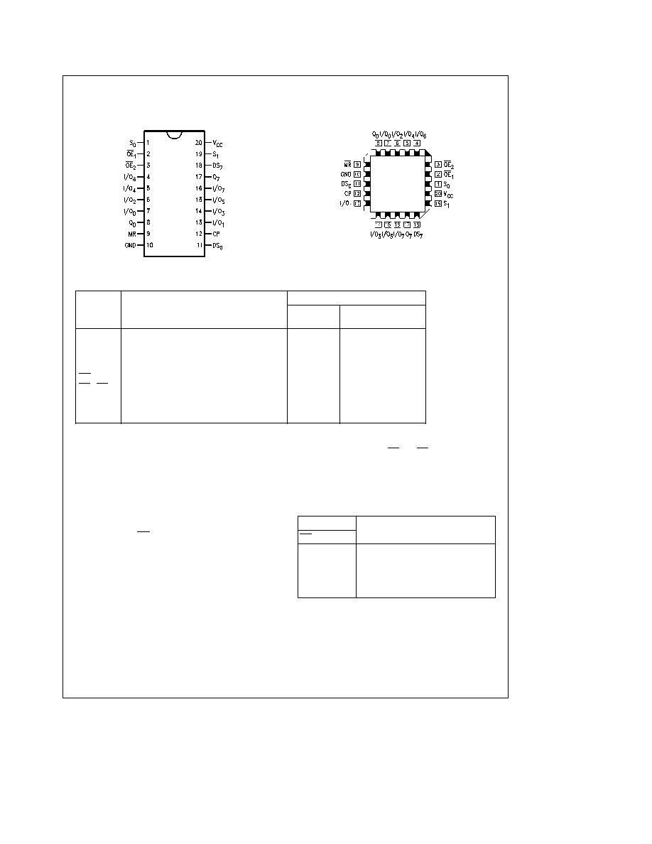
Connection Diagrams
Pin Assignment
for DIP SOIC and Flatpak
TL F 9515 ≠ 2
Pin Assignment
for LCC
TL F 9515 ≠ 3
Unit Loading Fan Out
54F 74F
Pin Names
Description
U L
Input I
IH
I
IL
HIGH LOW
Output I
OH
I
OL
CP
Clock Pulse Input (Active Rising Edge)
1 0 1 0
20 mA
b
0 6 mA
DS
0
Serial Data Input for Right Shift
1 0 1 0
20 mA
b
0 6 mA
DS
7
Serial Data Input for Left Shift
1 0 1 0
20 mA
b
0 6 mA
S
0
S
1
Mode Select Inputs
1 0 2 0
20 mA
b
1 2 mA
MR
Asynchronous Master Reset Input (Active LOW)
1 0 1 0
20 mA
b
0 6 mA
OE
1
OE
2
TRI-STATE Output Enable Inputs (Active LOW)
1 0 1 0
20 mA
b
0 6 mA
I O
0
≠ I O
7
Parallel Data Inputs or
3 5 1 083
70 mA
b
0 65 mA
TRI-STATE Parallel Outputs
150 40(33 3)
b
3 mA 24 mA (20 mA)
Q
0
Q
7
Serial Outputs
50 33 3
b
1 mA 20 mA
Functional Description
The 'F299 contains eight edge-triggered D-type flip-flops
and the interstage logic necessary to perform synchronous
shift left shift right parallel load and hold operations The
type of operation is determined by S
0
and S
1
as shown in
the Mode Select Table All flip-flop outputs are brought out
through TRI-STATE buffers to separate I O pins that also
serve as data inputs in the parallel load mode Q
0
and Q
7
are also brought out on other pins for expansion in serial
shifting of longer words
A LOW signal on MR overrides the Select and CP inputs
and resets the flip-flops All other state changes are initiated
by the rising edge of the clock Inputs can change when the
clock is in either state provided only that the recommended
setup and hold times relative to the rising edge of CP are
observed
A HIGH signal on either OE
1
or OE
2
disables the TRI-
STATE buffers and puts the I O pins in the high impedance
state In this condition the shift hold load and reset opera-
tions can still occur The TRI-STATE outputs are also dis-
abled by HIGH signals on both S
0
and S
1
in preparation for
a parallel load operation
Mode Select Table
Inputs
Response
MR S
1
S
0
CP
L
X
X
X
Asynchronous Reset Q
0
≠ Q
7
e
LOW
H
H
H
L Parallel Load I O
n
x
Q
n
H
L
H
L Shift Right DS
0
x
Q
0
Q
0
x
Q
1
etc
H
H
L
L Shift Left DS
7
x
Q
7
Q
7
x
Q
6
etc
H
L
L
X
Hold
H
e
HIGH Voltage Level
L
e
LOW Voltage Level
X
e
Immaterial
L
e
LOW-to-HIGH Clock Transition
2
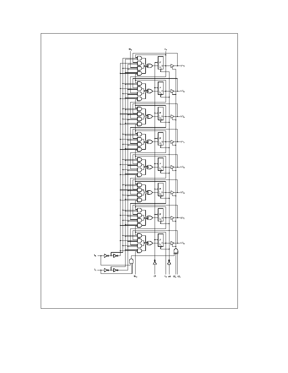
Logic Diagram
TL F 9515 ≠ 5
Please note that this diagram is provided only for the understanding of logic operations and should not be used to estimate propagation delays
3
Absolute Maximum Ratings
(Note 1)
If Military Aerospace specified devices are required
please contact the National Semiconductor Sales
Office Distributors for availability and specifications
Storage Temperature
b
65 C to
a
150 C
Ambient Temperature under Bias
b
55 C to
a
125 C
Junction Temperature under Bias
b
55 C to
a
175 C
Plastic
b
55 C to
a
150 C
V
CC
Pin Potential to
Ground Pin
b
0 5V to
a
7 0V
Input Voltage (Note 2)
b
0 5V to
a
7 0V
Input Current (Note 2)
b
30 mA to
a
5 0 mA
ESD Last Passing Voltage (Min)
4000V
Note 1
Absolute maximum ratings are values beyond which the device may
be damaged or have its useful life impaired Functional operation under
these conditions is not implied
Note 2
Either voltage limit or current limit is sufficient to protect inputs
Voltage Applied to Output
in HIGH State (with V
CC
e
0V)
Standard Output
b
0 5V to V
CC
TRI-STATE Output
b
0 5V to
a
5 5V
Current Applied to Output
in LOW State (Max)
twice the rated I
OL
(mA)
Recommended Operating
Conditions
Free Air Ambient Temperature
Military
b
55 C to
a
125 C
Commercial
0 C to
a
70 C
Supply Voltage
Military
a
4 5V to
a
5 5V
Commercial
a
4 5V to
a
5 5V
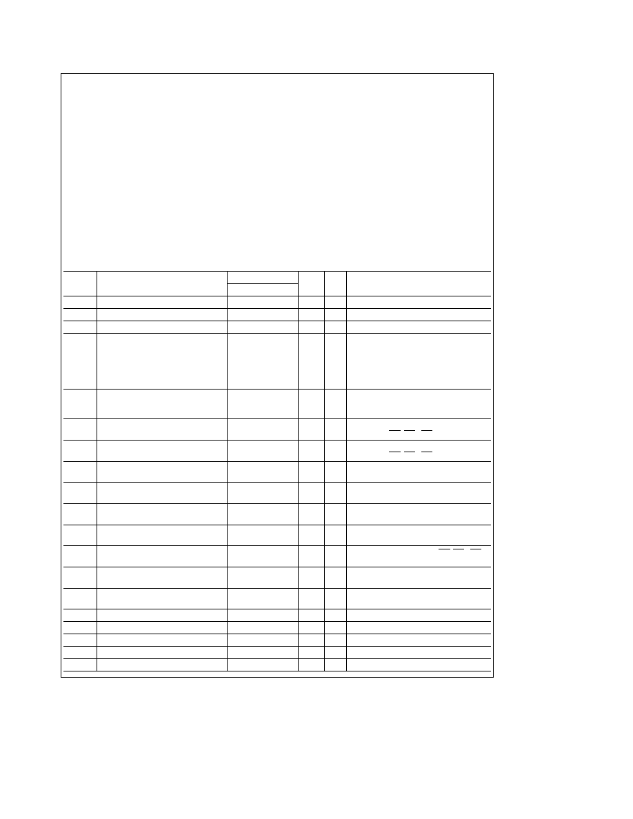
DC Electrical Characteristics
Symbol
Parameter
54F 74F
Units
V
CC
Conditions
Min
Typ
Max
V
IH
Input HIGH Voltage
2 0
V
Recognized as a HIGH Signal
V
IL
Input LOW Voltage
0 8
V
Recognized as a LOW Signal
V
CD
Input Clamp Diode Voltage
b
1 2
V
Min
I
IN
e b
18 mA
V
OH
Output HIGH
54F 10% V
CC
2 5
I
OH
e b
1 mA (Q
0
Q
7
I O
n
)
Voltage
54F 10% V
CC
2 4
I
OH
e b
3 mA (I O
n
)
74F 10% V
CC
2 5
V
Min
I
OH
e b
1 mA (Q
0
Q
7
I O
n
)
74F 10% V
CC
2 4
I
OH
e b
3 mA (I O
n
)
74F 5% V
CC
2 7
I
OH
e b
1 mA (Q
0
Q
7
I O
n
)
74F 5% V
CC
2 7
I
OH
e b
3 mA (I O
n
)
V
OL
Output LOW
54 10% V
CC
0 5
I
OL
e
20 mA
Voltage
74 10% V
CC
0 5
V
Min
I
OL
e
20 mA (Q
0
Q
7
)
74 10% V
CC
0 5
I
OL
e
24 mA (I O
n
)
I
IH
Input HIGH
54F
20 0
m
A
Max
V
IN
e
2 7V (CP DS
0
DS
7
S
0
S
1
Current
74F
5 0
MR OE
1
OE
2
)
I
BVI
Input HIGH Current
54F
100
m
A
Max
V
IN
e
7 0V (CP DS
0
DS
7
S
0
S
1
Breakdown Test
74F
7 0
MR OE
1
OE
2
)
I
BVIT
Input HIGH Current
54F
1 0
mA
Max
V
IN
e
5 5V (I O
n
)
Breakdown Test (I O)
74F
0 5
I
CEX
Output HIGH
54F
250
m
A
Max
V
OUT
e
V
CC
Leakage Current
74F
50
V
ID
Input Leakage
74F
4 75
V
0 0
I
ID
e
1 9 mA
Test
All Other Pins Grounded
I
OD
Output Leakage
74F
3 75
m
A
0 0
V
IOD
e
150 mV
Circuit Current
All Other Pins Grounded
I
IL
Input LOW Current
b
0 6
mA
Max
V
IN
e
0 5V (CP DS
0
DS
7
MR OE
1
OE
2
)
b
1 2
V
IN
e
0 5V (S
0
S
1
)
I
IH
a
Output Leakage Current
70
m
A
Max
V
I O
e
2 7V (I O
n
)
I
OZH
I
IL
a
Output Leakage Current
b
650
m
A
Max
V
I O
e
0 5V (I O
n
)
I
OZL
I
OS
Output Short-Circuit Current
b
60
b
150
mA
Max
V
OUT
e
0V
I
ZZ
Bus Drainage Test
500
m
A
0 0V
V
OUT
e
5 25V
I
CCH
Power Supply Current
68
95
mA
Max
V
O
e
HIGH
I
CCL
Power Supply Current
68
95
mA
Max
V
O
e
LOW
I
CCZ
Power Supply Current
68
95
mA
Max
V
O
e
HIGH Z
4
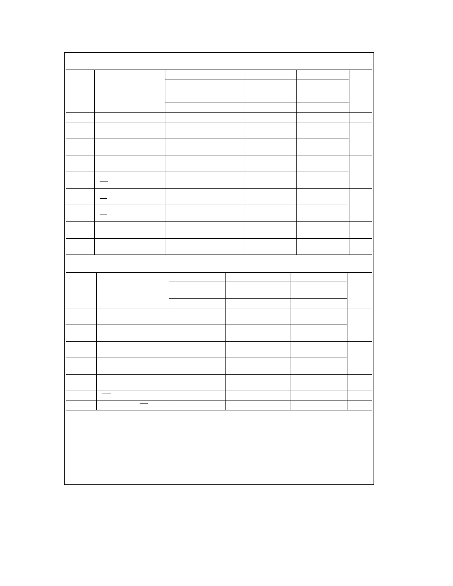
AC Electrical Characteristics
74F
54F
74F
T
A
e a
25 C
T
A
V
CC
e
Mil
T
A
V
CC
e
Com
Symbol
Parameter
V
CC
e a
5 0V
C
L
e
50 pF
C
L
e
50 pF
Units
C
L
e
50 pF
Min
Typ
Max
Min
Max
Min
Max
f
max
Maximum Input Frequency
70
100
85
70
MHz
t
PLH
Propagation Delay
4 0
7 0
8 0
4 0
9 0
4 0
8 5
t
PHL
CP to Q
0
or Q
7
4 5
6 5
8 0
4 5
9 5
4 5
8 5
ns
t
PLH
Propagation Delay
3 5
7 0
9 0
3 5
10 0
3 5
10 0
t
PHL
CP to I O
n
4 0
8 5
9 0
4 0
11 0
4 0
10 0
t
PHL
Propagation Delay
5 5
7 5
9 5
5 5
12 5
5 5
10 5
MR to Q
0
or Q
7
ns
t
PHL
Propagation Delay
5 5
11 0
10 0
5 5
12 0
5 5
10 5
MR to I O
n
t
PZH
Output Enable Time
3 5
6 0
8 0
3 0
9 5
3 5
9 0
t
PZL
OE to I O
n
4 0
7 0
10 0
4 0
13 0
4 0
11 0
ns
t
PHZ
Output Disable Time
2 0
4 5
6 0
1 5
7 0
2 0
7 0
t
PLZ
OE to I O
n
1 0
4 0
5 5
1 0
6 5
1 0
6 5
t
PZH
Output Enable Time
3 5
9 0
3 0
10 5
3 5
10 0
ns
t
PZL
S
n
to I O
n
4 0
10 0
4 0
13 0
4 0
11 0
t
PHZ
Output Disable Time
2 5
6 0
1 5
7 0
2 5
7 0
ns
t
PLZ
S
n
to I O
n
1 5
5 5
1 0
6 5
1 5
6 5
AC Operating Requirements
74F
54F
74F
Symbol
Parameter
T
A
e a
25 C
T
A
V
CC
e
Mil
T
A
V
CC
e
Com
Units
V
CC
e a
5 0V
Min
Max
Min
Max
Min
Max
t
s
(H)
Setup Time HIGH or LOW
8 5
10 0
8 5
t
s
(L)
S
0
or S
1
to CP
8 5
7 5
8 5
ns
t
h
(H)
Hold Time HIGH or LOW
0
0
0
t
h
(L)
S
0
or S
1
to CP
0
0
0
t
s
(H)
Setup Time HIGH or LOW
5 0
5 0
5 0
t
s
(L)
I O
n
DS
0
or DS
7
to CP
5 0
5 0
5 0
ns
t
h
(H)
Hold Time HIGH or LOW
2 0
2 0
2 0
t
h
(L)
I O
n
DS
0
or DS
7
to CP
2 0
2 0
2 0
t
w
(H)
CP Pulse Width
5 0
5 0
5 0
ns
t
w
(L)
HIGH or LOW
5 0
5 0
5 0
t
w
(L)
MR Pulse Width LOW
5 0
6 0
5 0
ns
t
rec
Recovery Time MR to CP
7 0
12 0
7 0
ns
5
Ordering Information
The device number is used to form part of a simplified purchasing code where the package type and temperature range are
defined as follows
74F
299
S
C
X
Temperature Range Family
Special Variations
74F
e
Commercial
QB
e
Military grade device with
54F
e
Military
environmental and burn-in
processing
Device Type
X
e
Devices shipped in 13 reel
Package Code
Temperature Range
P
e
Plastic DIP
C
e
Commercial (0 C to
a
70 C)
D
e
Ceramic DIP
M
e
Military (
b
55 C to
a
125 C)
S
e
Small Outline SOIC JEDEC
SJ
e
Small Outline SOIC EIAJ
F
e
Flatpak
L
e
Leadless Chip Carrier (LCC)
Physical Dimensions
inches (millimeters)
20-Lead Ceramic Leadless Chip Carrier (L)
NS Package Number E20A
6

Physical Dimensions
inches (millimeters) (Continued)
20-Lead Ceramic Dual-In-Line Package (D)
NS Package Number J20A
20-Lead (0 300 Wide) Molded Small Outline Package JEDEC (S)
NS Package Number M20B
7

Physical Dimensions
inches (millimeters) (Continued)
20-Lead (0 300 Wide) Molded Small Outline Package EIAJ (SJ)
NS Package Number MD20D
20-Lead (0 300 Wide) Molded Dual-In-Line Package (P)
NS Package Number N20A
8

9
54F74F299
Octal
Universal
ShiftStorage
Register
with
Common
Parallel
IO
Pins
Physical Dimensions
inches (millimeters) (Continued)
20-Lead Cerpack
NS Package Number W20A
LIFE SUPPORT POLICY
NATIONAL'S PRODUCTS ARE NOT AUTHORIZED FOR USE AS CRITICAL COMPONENTS IN LIFE SUPPORT
DEVICES OR SYSTEMS WITHOUT THE EXPRESS WRITTEN APPROVAL OF THE PRESIDENT OF NATIONAL
SEMICONDUCTOR CORPORATION As used herein
1 Life support devices or systems are devices or
2 A critical component is any component of a life
systems which (a) are intended for surgical implant
support device or system whose failure to perform can
into the body or (b) support or sustain life and whose
be reasonably expected to cause the failure of the life
failure to perform when properly used in accordance
support device or system or to affect its safety or
with instructions for use provided in the labeling can
effectiveness
be reasonably expected to result in a significant injury
to the user
National Semiconductor
National Semiconductor
National Semiconductor
National Semiconductor
National Semiconductores
National Semiconductor
Corporation
GmbH
Japan Ltd
Hong Kong Ltd
Do Brazil Ltda
(Australia) Pty Ltd
2900 Semiconductor Drive
Livry-Gargan-Str 10
Sumitomo Chemical
13th Floor Straight Block
Rue Deputado Lacorda Franco
Building 16
P O Box 58090
D-82256 F4urstenfeldbruck
Engineering Center
Ocean Centre 5 Canton Rd
120-3A
Business Park Drive
Santa Clara CA 95052-8090
Germany
Bldg 7F
Tsimshatsui Kowloon
Sao Paulo-SP
Monash Business Park
Tel 1(800) 272-9959
Tel (81-41) 35-0
1-7-1 Nakase Mihama-Ku
Hong Kong
Brazil 05418-000
Nottinghill Melbourne
TWX (910) 339-9240
Telex 527649
Chiba-City
Tel (852) 2737-1600
Tel (55-11) 212-5066
Victoria 3168 Australia
Fax (81-41) 35-1
Ciba Prefecture 261
Fax (852) 2736-9960
Telex 391-1131931 NSBR BR
Tel (3) 558-9999
Tel (043) 299-2300
Fax (55-11) 212-1181
Fax (3) 558-9998
Fax (043) 299-2500
National does not assume any responsibility for use of any circuitry described no circuit patent licenses are implied and National reserves the right at any time without notice to change said circuitry and specifications