
TL F 9545
54F74F521
8-Bit
Identity
Comparator
May 1995
54F 74F521
8-Bit Identity Comparator
General Description
The 'F521 is an expandable 8-bit comparator It compares
two words of up to eight bits each and provides a LOW
output when the two words match bit for bit The expansion
input I
AeB
also serves as an active LOW enable input
Features
Y
Compares two 8-bit words in 6 5 ns typ
Y
Expandable to any word length
Y
20-pin package
Commercial
Military
Package
Package Description
Number
74F521PC
N20A
20-Lead (0 300 Wide) Molded Dual-In-Line
54F521DM (Note 2)
J20A
20-Lead Ceramic Dual-In-Line
74F521SC (Note 1)
M20B
20-Lead (0 300 Wide) Molded Small Outline JEDEC
74F521SJ (Note 1)
M20D
20-Lead (0 300 Wide) Molded Small Outline EIAJ
74F521MSA (Note 1)
MSA20
20-Lead Molded Shrink Small Outline EIAJ type II
Note 1
Devices also available in 13
reel Use suffix
e
SCX SJX and MSAX
Note 2
Military grade device with environmental and burn-in processing Use suffix
e
DMQB
Logic Symbols
TL F 9545 � 1
IEEE IEC
TL F 9545 � 4
TRI-STATE
is a registered trademark of National Semiconductor Corporation
C1995 National Semiconductor Corporation
RRD-B30M75 Printed in U S A
Unit Loading Fan Out
54F 74F
Pin Names
Description
U L
Input I
IH
I
IL
HIGH LOW
Output I
OH
I
OL
A
0
� A
7
Word A Inputs
1 0 1 0
20 mA
b
0 6 mA
B
0
� B
7
Word B Inputs
1 0 1 0
20 mA
b
0 6 mA
I
AeB
Expansion or Enable Input (Active LOW)
1 0 1 0
20 mA
b
0 6 mA
O
AeB
Identity Output (Active LOW)
50 33 3
b
1 mA 20 mA
Truth Table
Inputs
Output
I
A e B
A B
O
A e B
L
A
e
B
L
L
A
i
B
H
H
A
e
B
H
H
A
i
B
H
H
e
HIGH Voltage Level
L
e
LOW Voltage Level
A
0
e
B
0
A
1
e
B
1
A
2
e
B
2
etc
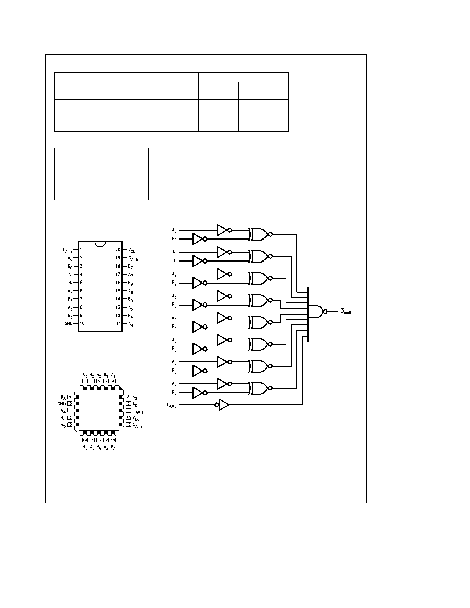
Connection Diagrams
Pin Assignment for DIP
SOIC SSOP and Flatpak
TL F 9545 � 2
Pin Assignment
for LCC
TL F 9545 � 3
Logic Diagram
TL F 9545 � 5
Please note that this diagram is provided only for the understanding of logic operations and should not be
used to estimate propagation delays
2

Absolute Maximum Ratings
(Note 1)
If Military Aerospace specified devices are required
please contact the National Semiconductor Sales
Office Distributors for availability and specifications
Storage Temperature
b
65 C to
a
150 C
Ambient Temperature under Bias
b
55 C to
a
125 C
Junction Temperature under Bias
b
55 C to
a
175 C
Plastic
b
55 C to
a
150 C
V
CC
Pin Potential to
Ground Pin
b
0 5V to
a
7 0V
Input Voltage (Note 2)
b
0 5V to
a
7 0V
Input Current (Note 2)
b
30 mA to
a
5 0 mA
Voltage Applied to Output
in HIGH State (with V
CC
e
0V)
Standard Output
b
0 5V to V
CC
TRI-STATE Output
b
0 5V to
a
5 5V
Current Applied to Output
in LOW State (Max)
twice the rated I
OL
(mA)
Note 1
Absolute maximum ratings are values beyond which the device may
be damaged or have its useful life impaired Functional operation under
these conditions is not implied
Note 2
Either voltage limit or current limit is sufficient to protect inputs
Recommended Operating
Conditions
Free Air Ambient Temperature
Military
b
55 C to
a
125 C
Commercial
0 C to
a
70 C
Supply Voltage
Military
a
4 5V to
a
5 5V
Commercial
a
4 5V to
a
5 5V
DC Electrical Characteristics
Symbol
Parameter
54F 74F
Units
V
CC
Conditions
Min
Typ
Max
V
IH
Input HIGH Voltage
2 0
V
Recognized as a HIGH Signal
V
IL
Input LOW Voltage
0 8
V
Recognized as a LOW Signal
V
CD
Input Clamp Diode Voltage
b
1 2
V
Min
I
IN
e b
18 mA
V
OH
Output HIGH
54F 10% V
CC
2 5
I
OH
e b
1 mA
Voltage
74F 10% V
CC
2 5
V
Min
I
OH
e b
1 mA
74F 5% V
CC
2 7
I
OH
e b
1 mA
V
OL
Output LOW
54F 10% V
CC
0 5
V
Min
I
OL
e
20 mA
Voltage
74F 10% V
CC
0 5
I
OL
e
20 mA
I
IH
Input HIGH
54F
20 0
m
A
Max
V
IN
e
2 7V
Current
74F
5 0
I
BVI
Input HIGH Current
54F
100
m
A
Max
V
IN
e
7 0V
Breakdown Test
74F
7 0
I
CEX
Output HIGH
54F
250
m
A
Max
V
OUT
e
V
CC
Leakage Current
74F
50
V
ID
Input Leakage
74F
4 75
V
0 0
I
ID
e
1 9 mA
Test
All Other Pins Grounded
I
OD
Output Leakage
74F
3 75
m
A
0 0
V
IOD
e
150 mV
Circuit Current
All Other Pins Grounded
I
IL
Input LOW Current
b
0 6
mA
Max
V
IN
e
0 5V
I
OS
Output Short-Circuit Current
b
60
b
150
mA
Max
V
OUT
e
0V
I
CCH
Power Supply Current
21
32
mA
Max
V
O
e
HIGH
3

AC Electrical Characteristics
74F
54F
74F
T
A
e a
25 C
T
A
V
CC
e
Mil
T
A
V
CC
e
Com
Symbol
Parameter
V
CC
e a
5 0V
C
L
e
50 pF
C
L
e
50 pF
Units
C
L
e
50 pF
Min
Typ
Max
Min
Max
Min
Max
t
PLH
Propagation Delay
3 0
7 0
10 0
3 0
14 0
3 0
11 0
ns
t
PHL
A
n
or B
n
to O
AeB
4 5
7 0
10 0
4 0
15 0
4 0
11 0
t
PLH
Propagation Delay
3 0
5 0
6 5
3 0
8 5
3 0
7 5
ns
t
PHL
I
AeB
to O
AeB
3 5
6 5
9 0
3 5
13 5
3 5
10 0
Applications
Ripple Expansion
TL F 9545 � 6
Parallel Expansion
TL F 9545 � 7
Ordering Information
The device number is used to form part of a simplified purchasing code where the package type and temperature range are
defined as follows
74F
521
S
C
X
Temperature Range Family
Special Variations
74F
e
Commercial
QB
e
Military grade device with
54F
e
Military
environmental and burn-in
processing
Device Type
X
e
Devices shipped in 13 reel
Package Code
Temperature Range
P
e
Plastic DIP
C
e
Commercial (0 C to
a
70 C)
D
e
Ceramic DIP
M
e
Military (
b
55 C to
a
125 C)
F
e
Flatpak
NOTE
S
e
Small Outline SOIC JEDEC
Not required for MSA package code
SJ
e
Small Outline SOIC EIAJ
MSA
e
Shrink Small Outline (EIAJ SSOP)
4

Physical Dimensions
inches (millimeters)
20-Lead Ceramic Dual-In-Line Package (D)
NS Package Number J20A
20-Lead (0 300 Wide) Molded Small Outline Package JEDEC (S)
NS Package Number M20B
5