
TL F 9596
54F74F823
9-Bit
D-Type
Flip-Flop
December 1994
54F 74F823
9-Bit D-Type Flip-Flop
General Description
The 'F823 is a 9-bit buffered register It features Clock En-
able and Clear which are ideal for parity bus interfacing in
high performance microprogramming systems
The 'F823 is functionally and pin compatible with AMD's
Am29823
Features
Y
TRI-STATE
outputs
Y
Clock Enable and Clear
Y
Direct replacement for AMD's Am29823
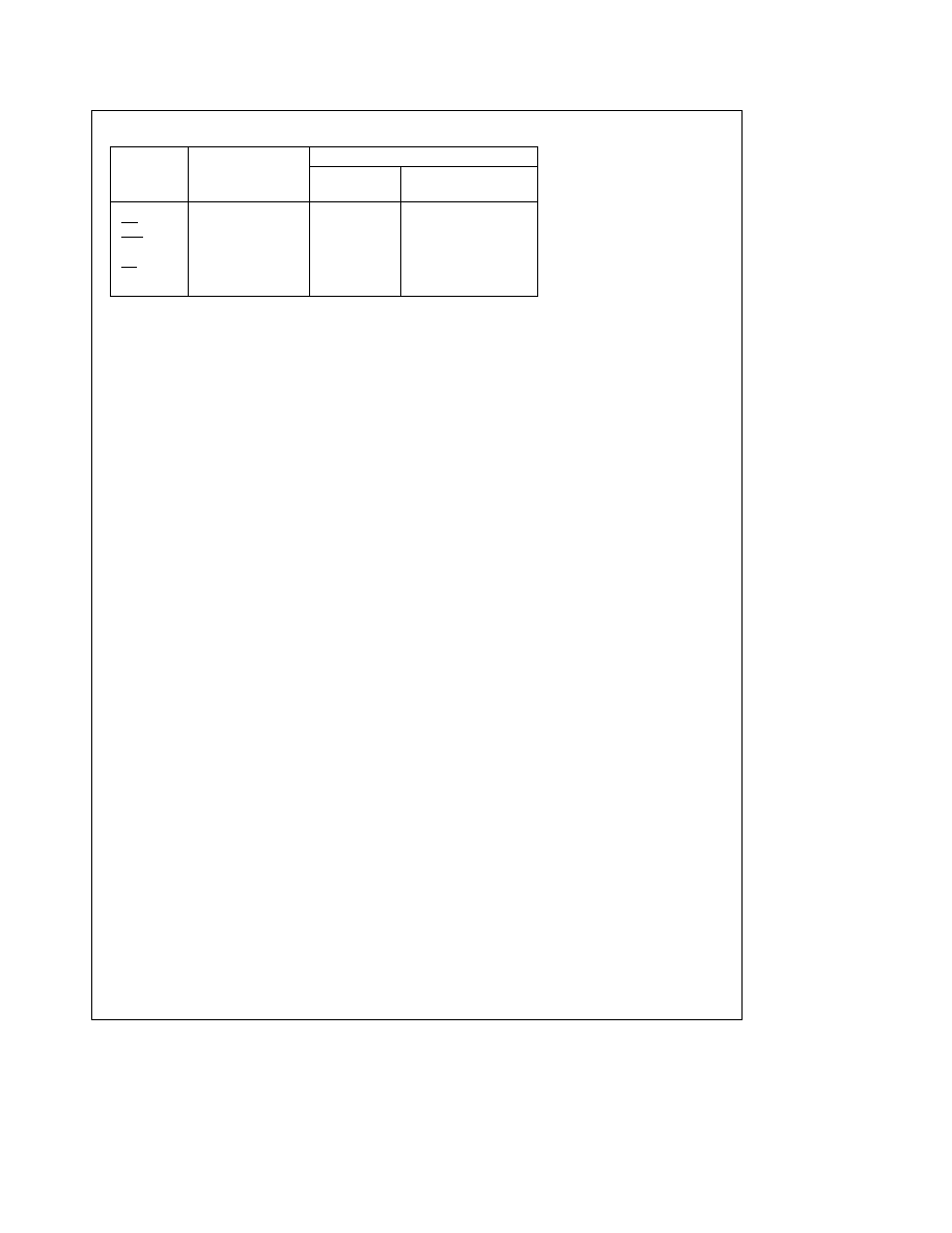
Commercial
Military
Package
Package Description
Number
74F823SPC
N24C
24-Lead (0 300 Wide) Molded Dual-In-Line
54F823SDM (Note 2)
J24F
24-Lead (0 300 Wide) Ceramic Dual-In-Line
74F823SC (Note 1)
M24B
24-Lead (0 300 Wide) Molded Small Outline JEDEC
54F823FM (Note 2)
W24C
24-Lead Cerpack
54F823LM (Note 2)
E28A
24-Lead Ceramic Chip Carrier Type C
Note 1
Devices also available in 13
reel Use suffix
e
SCX
Note 2
Military grade device with environmental and burn-in processing Use suffix
e
SDMQB FMQB and LMQB
Logic Symbols
Connection Diagrams
TL F 9596 � 2
IEEE IEC
TL F 9596 � 1
Pin Assignment for
DIP SOIC and Flatpak
TL F 9596 � 3
Pin Assignment
for LCC
TL F 9596 � 4
TRI-STATE
is a registered trademark of National Semiconductor Corporation
C1995 National Semiconductor Corporation
RRD-B30M75 Printed in U S A
Unit Loading Fan Out
Pin Names
Description
54F 74F
U L
Input I
IH
I
IL
HIGH LOW
Output I
OH
I
OL
D
0
� D
8
Data Inputs
1 0 1 0
20 mA
b
0 6 mA
OE
Output Enable Input
1 0 1 0
20 mA
b
0 6 mA
CLR
Clear
1 0 1 0
20 mA
b
0 6 mA
CP
Clock Input
1 0 2 0
20 mA
b
1 2 mA
EN
Clock Enable
1 0 1 0
20 mA
b
0 6 mA
O
0
� O
8
TRI-STATE Outputs
150 40 (33 3)
b
3 mA 24 mA (20 mA)
2

Functional Description
The 'F823 device consists of nine D-type edge-triggered
flip-flops It has TRI-STATE true outputs and is organized in
broadside pinning The buffered Clock (CP) and buffered
Output Enable (OE) are common to all flip-flops The flip-
flops will store the state of their individual D inputs that meet
the setup and hold times requirements on the LOW-to-HIGH
CP transition With the OE LOW the contents of the flip-
flops are available at the outputs When the OE is HIGH the
outputs go to the high impedance state Operation of the
OE input does not affect the state of the flip-flops In addi-
tion to the Clock and Output Enable pins the 'F823 has
Clear (CLR) and Clock Enable (EN) pins
When the CLR is LOW and the OE is LOW the outputs are
LOW When CLR is HIGH data can be entered into the flip-
flops When EN is LOW data on the inputs is transferred to
the outputs on the LOW to HIGH clock transition When the
EN is HIGH the outputs do not change state regardless of
the data or clock inputs transitions This device is ideal for
parity bus interfacing in high performance systems
Function Table
Inputs
Internal
Output
Function
OE
CLR
EN
CP
D
Q
O
H
H
L
H
X
NC
Z
Hold
H
H
L
L
X
NC
Z
Hold
H
H
H
X
X
NC
Z
Hold
L
H
H
X
X
NC
NC
Hold
H
L
X
X
X
H
Z
Clear
L
L
X
X
X
H
L
Clear
H
H
L
L
H
H
Z
Load
H
H
L
L
H
L
Z
Load
L
H
L
L
L
H
L
Data Available
L
H
L
L
H
L
H
Data Available
L
H
L
H
X
NC
NC
No Change in Data
L
H
L
L
X
NC
NC
No Change in Data
L
e
LOW Voltage Level
H
e
HIGH Voltage Level
X
e
Immaterial
Z
e
High Impedance
L
e
LOW-to-HIGH Transition
NC
e
No Change
Logic Diagram
TL F 9596 � 5
Please note that this diagram is provided only for the understanding of logic operations and should not be used to estimate propagation delays
3

Absolute Maximum Ratings
(Note 1)
If Military Aerospace specified devices are required
please contact the National Semiconductor Sales
Office Distributors for availability and specifications
Storage Temperature
b
65 C to
a
150 C
Ambient Temperature under Bias
b
55 C to
a
125 C
Junction Temperature under Bias
b
55 C to
a
175 C
Plastic
b
55 C to
a
150 C
V
CC
Pin Potential to
Ground Pin
b
0 5V to
a
7 0V
Input Voltage (Note 2)
b
0 5V to
a
7 0V
Input Current (Note 2)
b
30 mA to
a
5 0 mA
Voltage Applied to Output
in HIGH State (with V
CC
e
0V)
Standard Output
b
0 5V to V
CC
TRI-STATE Output
b
0 5V to
a
5 5V
Current Applied to Output
in LOW State (Max)
twice the rated I
OL
(mA)
Note 1
Absolute maximum ratings are values beyond which the device may
be damaged or have its useful life impaired Functional operation under
these conditions is not implied
Note 2
Either voltage limit or current limit is sufficient to protect inputs
Recommended Operating
Conditions
Free Air Ambient Temperature
Military
b
55 C to
a
125 C
Commercial
0 C to
a
70 C
Supply Voltage
Military
a
4 5V to
a
5 5V
Commercial
a
4 5V to
a
5 5V
DC Electrical Characteristics
Symbol
Parameter
54F 74F
Units
V
CC
Conditions
Min
Typ
Max
V
IH
Input HIGH Voltage
2 0
V
Recognized as a HIGH Signal
V
IL
Input LOW Voltage
0 8
V
Recognized as a LOW Signal
V
CD
Input Clamp Diode Voltage
b
1 2
V
Min
I
IN
e b
18 mA
V
OH
54F 10% V
CC
2 5
I
OH
e b
1 mA
54F 10% V
CC
2 4
I
OH
e b
3 mA
Output HIGH
74F 10% V
CC
2 5
V
Min
I
OH
e b
1 mA
Voltage
74F 10% V
CC
2 4
I
OH
e b
3 mA
74F 5% V
CC
2 7
I
OH
e b
1 mA
74F 5% V
CC
2 7
I
OH
e b
3 mA
V
OL
Output LOW
54F 10% V
CC
0 5
V
Min
I
OL
e
20 mA
Voltage
74F 10% V
CC
0 5
I
OL
e
24 mA
I
IH
Input HIGH
54F
20 0
m
A
Max
V
IN
e
2 7V
Current
74F
5 0
I
BVI
Input HIGH Current
54F
100
m
A
Max
V
IN
e
7 0V
Breakdown Test
74F
7 0
I
CEX
Output HIGH
54F
250
m
A
Max
V
OUT
e
V
CC
Leakage Current
74F
50
V
ID
Input Leakage
74F
4 75
V
0 0
I
ID
e
1 9 mA
Test
All Other Pins Grounded
I
OD
Output Leakage
74F
3 75
m
A
0 0
V
IOD
e
150 mV
Circuit Current
All Other Pins Grounded
I
IL
Input LOW
b
0 6
mA
Max
V
IN
e
0 5V (OE CLR EN)
Current
b
1 2
mA
Max
V
IN
e
0 5V (CP)
I
OZH
Output Leakage Current
50
m
A
Max
V
OUT
e
2 7V
I
OZL
Output Leakage Current
b
50
m
A
Max
V
OUT
e
0 5V
I
OS
Output Short-Circuit Current
b
60
b
150
mA
Max
V
OUT
e
0V
I
ZZ
Buss Drainage Test
500
m
A
0 0V
V
OUT
e
5 25V
I
CCZ
Power Supply Current
75
100
mA
Max
V
O
e
HIGH Z
4

AC Electrical Characteristics
74F
54F
74F
T
A
e a
25 C
T
A
V
CC
e
Mil
T
A
V
CC
e
Com
Symbol
Parameter
V
CC
e a
5 0V
C
L
e
50 pF
C
L
e
50 pF
Units
C
L
e
50 pF
Min
Typ
Max
Min
Max
Min
Max
f
max
Maximum Clock Frequency
100
160
60
70
MHz
t
PLH
Propagation Delay
2 0
5 6
9 5
2 0
10 5
2 0
10 5
ns
t
PHL
CP to O
n
2 0
5 2
9 5
2 0
10 5
2 0
10 5
t
PHL
Propagation Delay
4 0
7 1
12 0
4 0
13 0
4 0
13 0
ns
CLR to O
n
t
PZH
Output Enable Time
2 0
5 8
10 5
2 0
13 0
2 0
11 5
t
PZL
OE to O
n
2 0
5 5
10 5
2 0
13 0
2 0
11 5
ns
t
PHZ
Output Disable Time
1 5
2 9
7 0
1 0
7 5
1 5
7 5
t
PLZ
OE to O
n
1 5
2 7
7 0
1 0
7 5
1 5
7 5
AC Operating Requirements
74F
54F
74F
Symbol
Parameter
T
A
e a
25 C
T
A
V
CC
e
Mil
T
A
V
CC
e
Com
Units
V
CC
e a
5 0V
Min
Max
Min
Max
Min
Max
t
s
(H)
Setup Time HIGH or LOW
2 5
4 0
3 0
t
s
(L)
D
n
to CP
2 5
4 0
3 0
ns
t
h
(H)
Hold Time HIGH or LOW
2 5
2 5
2 5
t
h
(L)
D
n
to CP
2 5
2 5
2 5
t
s
(H)
Setup Time HIGH or LOW
4 5
5 0
5 0
t
s
(L)
EN to CP
2 5
3 0
3 0
ns
t
h
(H)
Hold Time HIGH or LOW
2 0
3 0
2 0
t
h
(L)
EN to CP
0
1 0
0
t
w
(H)
CP Pulse Width
5 0
6 0
6 0
ns
t
w
(L)
HIGH or LOW
5 0
6 0
6 0
t
w
(L)
CLR Pulse Width LOW
5 0
5 0
5 0
ns
t
rec
CLR Recovery Time
5 0
5 0
5 0
ns
Ordering Information
The device number is used to form part of a simplified purchasing code where the package type and temperature range are
defined as follows
74F
823
S
C
X
Temperature Range Family
Special Variations
74F
e
Commercial
QB
e
Military grade device with
54F
e
Military
environmental and burn-in
processing
Device Type
Temperature Range
Package Code
C
e
Commercial (0 C to
a
70 C)
SP
e
Slim Plastic DIP
M
e
Military (
b
55 C to
a
125 C)
SD
e
Slim Ceramic DIP
F
e
Flatpak
L
e
Leadless Chip Carrier (LCC)
S
e
Small Outline (SOIC)
5