 | –≠–ª–µ–∫—Ç—Ä–æ–Ω–Ω—ã–π –∫–æ–º–ø–æ–Ω–µ–Ω—Ç: 54FCT138F | –°–∫–∞—á–∞—Ç—å:  PDF PDF  ZIP ZIP |

54FCT138
1-of-8 Decoder/Demultiplexer
General Description
The FCT138 is a high-speed 1-of-8 decoder/demultiplexer.
This device is ideally suited for high-speed bipolar memory
chip select address decoding. The multiple input enables al-
low parallel expansion to a 1-of-24 decoder using just three
FCT138 devices or a 1-of-32 decoder using four FCT138 de-
vices and one inverter.
Features
n
Demultiplexing capability
n
Multiple input enable for easy expansion
n
Active LOW mutually exclusive outputs
n
Outputs sink capability of 32mA, source capability of
12mA
n
TTL input and output level compatible
n
CMOS power consumption
n
Standard Microcircuit Drawing (SMD) 5962-8765401
Ordering Code
Military
Package
Package Description
Number
54FCT138DMQB
J16A
16-Lead Ceramic Dual-In-Line
54FCT138FMQB
W16A
16-Lead Cerpack
54FCT138LMQB
E20A
20-Lead Ceramic Leadless Chip Carrier, Type C
Logic Symbols
Pin Names
Description
A
0
≠A
2
Address Inputs
E
1
≠E
2
Enable Inputs
E
3
Enable Input
O
0
≠O
7
Outputs
Connection Diagrams
FACT
Æ
is a registered trademark of Fairchild Semiconductor Corporation.
DS100963-1
IEEE/IEC
DS100963-7
Pin Assignment
for DIP and Flatpak
DS100963-2
Pin Assignment
for LCC
DS100963-3
October 1999
54FCT138
1-of-8
Decoder/Demultiplexer
© 1999 National Semiconductor Corporation
DS100963
www.national.com
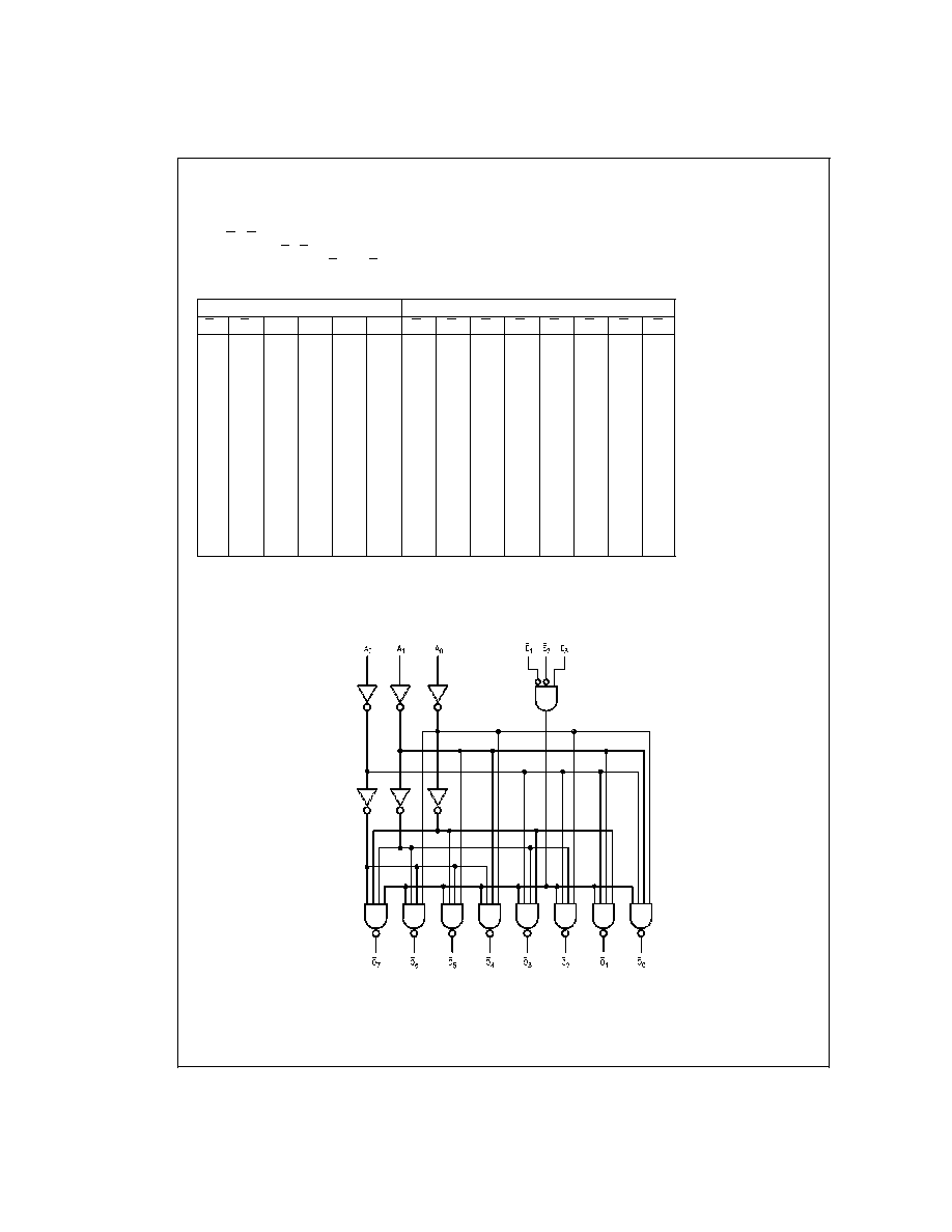
Functional Description
The FCT138 high-speed 1-of-8 decoder/demultiplexer ac-
cepts three binary weighted inputs (A
0
, A
1
, A
2
) and, when
enabled, provides eight mutually exclusive active-LOW out-
puts (O
0
≠O
7
). The FCT138 features three Enable inputs,
two active-LOW (E
1
, E
2
) and one active-HIGH (E
3
). All out-
puts will be HIGH unless E
1
and E
2
are LOW and E
3
is
HIGH. This multiple enable function allows easy parallel ex-
pansion of the device to a 1-of-32 (5 lines to 32 lines) de-
coder with just four FCT138 devices and one inverter (see
Figure 1). The FCT138 can be used as an 8-output demulti-
plexer by using one of the active LOW Enable inputs as the
data input and the other Enable inputs as strobes. The En-
able inputs which are not used must be permanently tied to
their appropriate active-HIGH or active-LOW state.
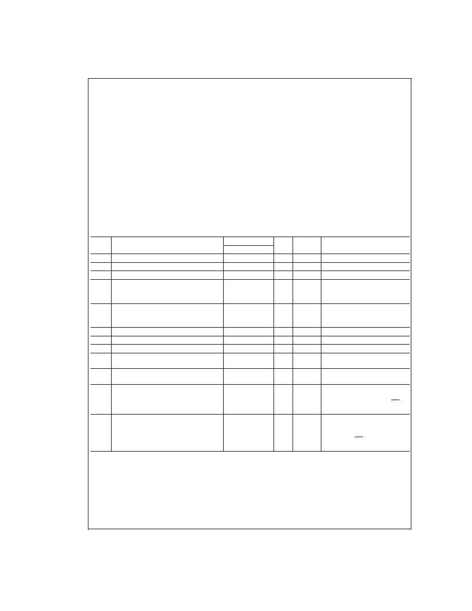
Inputs
Outputs
E
1
E
2
E
3
A
0
A
1
A
2
O
0
O
1
O
2
O
3
O
4
O
5
O
6
O
7
H
X
X
X
X
X
H
H
H
H
H
H
H
H
X
H
X
X
X
X
H
H
H
H
H
H
H
H
X
X
L
X
X
X
H
H
H
H
H
H
H
H
L
L
H
L
L
L
L
H
H
H
H
H
H
H
L
L
H
H
L
L
H
L
H
H
H
H
H
H
L
L
H
L
H
L
H
H
L
H
H
H
H
H
L
L
H
H
H
L
H
H
H
L
H
H
H
H
L
L
H
L
L
H
H
H
H
H
L
H
H
H
L
L
H
H
L
H
H
H
H
H
H
L
H
H
L
L
H
L
H
H
H
H
H
H
H
H
L
H
L
L
H
H
H
H
H
H
H
H
H
H
H
L
H = HIGH Voltage Level
L = LOW Voltage Level
X = Immaterial
Logic Diagram
DS100963-4
Please note that this diagram is provided only for the understanding of logic operations and should not be used to estimate propagation delays.
54FCT138
www.national.com
2
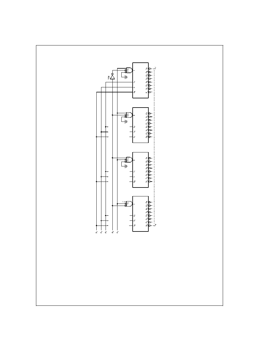
Logic Diagram
(Continued)
DS100963-5
FIGURE
1.
Expansion
to
1-of-32
Decoding
54FCT138
www.national.com
3
Absolute Maximum Ratings
(Note 1)
If Military/Aerospace specified devices are required,
please contact the National Semiconductor Sales Office/
Distributors for availability and specifications.
Storage Temperature
-65∞C to +150∞C
Ambient Temperature under Bias
-55∞C to +125∞C
Junction Temperature under Bias
Ceramic
-55∞C to +175∞C
V
CC
Pin Potential to
Ground Pin
-0.5V to +7.0V
Input Voltage (Note 1)
-0.5V to +7.0V
Input Current (Note 1)
-30 mA to +5.0 mA
Voltage Applied to Any Output
in the Disabled or
Power-Off State
-0.5V to +5.5V
in the HIGH State
-0.5V to V
CC
Current Applied to Output
in LOW State (Max)
Twice the rated I
OL
(mA)
DC Latchup Source Current
-500 mA
Recommended Operating
Conditions
Free Air Ambient Temperature
Military
-55∞C to +125∞C
Supply Voltage
Military
+4.5V to +5.5V
Minimum Input Edge Rate
(
V/
t)
Data Input
50 mV/ns
Enable Input
20 mV/ns
Note 1: Absolute maximum ratings are those values beyond which damage
to the device may occur. The databook specifications should be met, without
exception, to ensure that the system design is reliable over its power supply,
temperature, and output/input loading variables. National does not recom-
mend operation of FACT
Æ
circuits outside databook specifications.
DC Characteristics for 'FCT Family Devices
Symbol
Parameter
FCT138
Units
V
CC
Conditions
Min
Max
V
IH
Input HIGH Voltage
2.0
V
Recognized HIGH Signal
V
IL
Input LOW Voltage
0.8
V
Recognized LOW Signal
V
CD
Input Clamp Diode Voltage
-1.2
V
Min
I
IN
= -18 mA
V
OH
Output HIGH
Voltage
54FCT
4.3
V
Min
I
OH
= -300 µA
54FCT
2.4
I
OH
= -12 mA
V
OL
Output LOW
Voltage
54FCT
0.2
V
Min
I
OL
= 300 µA
54FCT
0.5
I
OL
= 32 mA
I
IH
Input HIGH Current
5
µA
Max
V
IN
= V
CC
I
IL
Input LOW Current
-5
µA
Max
V
IN
= 0.0V
I
OS
Output Short-Circuit Current
-60
mA
Max
V
OUT
= 0.0V
I
CCQ
Quiescent Power Supply Current
1.5
mA
Max
V
IN
<
0.2V or V
IN
5.3V, V
CC
=
5.5V
I
CC
Quiescent Power
Supply Current
2.0
mA
Max
V
I
= 3.4V, V
CC
= 5.5V
I
CCD
Dynamic I
CC
0.4
mA/
MHz
Max
Outputs Open, V
CC
= 5.5V, V
IN
5.3V or V
IN
<
0.2V, One Bit
Toggling, 50% Duty Cycle, OE =
GND, LE = V
CC
I
CCT
Total Power Supply
Current
5.5
mA
Max
Outputs Open, f
CP
= 10 MHz,
V
CC
= 5.5V, V
IN
5.3V or V
IN
<
0.2V, One Bit Toggling, 50%
Duty Cycle, OE = GND, LE =
V
CC
Note 2: All outputs loaded; thresholds on input associated with output under test.
Note 3: Maximum test duration 2.0 ms, one output loaded at a time.
54FCT138
www.national.com
4

AC Electrical Characteristics
54FCT
V
CC
T
A
= -55∞C
Fig.
Symbol
Parameter
(V)
to +125∞C
Units
No.
(Note 4)
C
L
= 50 pF
Min
Max
t
PLH
Propagation Delay
5.0
1.0
12.0
ns
A
n
to O
n
t
PHL
Propagation Delay
5.0
1.0
12.0
ns
A
n
to O
n
t
PLH
Propagation Delay
5.0
1.0
12.5
ns
E
1
or E
2
to O
n
t
PHL
Propagation Delay
5.0
1.0
12.5
ns
E
1
or E
2
to O
n
t
PLH
Propagation Delay
5.0
1.0
12.5
ns
E
3
to O n
t
PHL
Propagation Delay
5.0
1.0
12.5
ns
E
3
to O n
Note 4: Voltage Range 5.0 is 5.0V
±
0.5V
Capacitance
Symbol
Parameter
Typ
Units
Conditions
C
IN
Input Capacitance
4.5
pF
V
CC
= OPEN
C
PD
Power Dissipation
60.0
pF
V
CC
= 5.0V
Capacitance
54FCT138
www.national.com
5

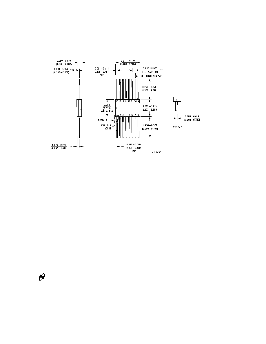
Physical Dimensions
inches (millimeters) unless otherwise noted
20 Terminal Ceramic Leadless Chip Carrier (L)
NS Package Number E20A
16 Lead Ceramic Dual-In-Line Package (D)
NS Package Number J16A
54FCT138
www.national.com
6
Physical Dimensions
inches (millimeters) unless otherwise noted (Continued)
LIFE SUPPORT POLICY
NATIONAL'S PRODUCTS ARE NOT AUTHORIZED FOR USE AS CRITICAL COMPONENTS IN LIFE SUPPORT
DEVICES OR SYSTEMS WITHOUT THE EXPRESS WRITTEN APPROVAL OF THE PRESIDENT AND GENERAL
COUNSEL OF NATIONAL SEMICONDUCTOR CORPORATION. As used herein:
1. Life support devices or systems are devices or
systems which, (a) are intended for surgical implant
into the body, or (b) support or sustain life, and
whose failure to perform when properly used in
accordance with instructions for use provided in the
labeling, can be reasonably expected to result in a
significant injury to the user.
2. A critical component is any component of a life
support device or system whose failure to perform
can be reasonably expected to cause the failure of
the life support device or system, or to affect its
safety or effectiveness.
National Semiconductor
Corporation
Americas
Tel: 1-800-272-9959
Fax: 1-800-737-7018
Email: support@nsc.com
National Semiconductor
Europe
Fax: +49 (0) 1 80-530 85 86
Email: europe.support@nsc.com
Deutsch Tel: +49 (0) 1 80-530 85 85
English
Tel: +49 (0) 1 80-532 78 32
FranÁais Tel: +49 (0) 1 80-532 93 58
Italiano
Tel: +49 (0) 1 80-534 16 80
National Semiconductor
Asia Pacific Customer
Response Group
Tel: 65-2544466
Fax: 65-2504466
Email: sea.support@nsc.com
National Semiconductor
Japan Ltd.
Tel: 81-3-5639-7560
Fax: 81-3-5639-7507
www.national.com
16 Lead Ceramic Flatpak (F)
NS Package Number W16A
54FCT138
1-of-8
Decoder/Demultiplexer
National does not assume any responsibility for use of any circuitry described, no circuit patent licenses are implied and National reserves the right at any time without notice to change said circuitry and specifications.