
TL F 6416
54LS253DM54LS253DM74LS253
TRI-STATE
Data
SelectorsMultiplexers
June 1989
54LS253 DM54LS253 DM74LS253
TRI-STATE
Data Selectors Multiplexers
General Description
Each of these Schottky-clamped data selectors multiplex-
ers contains inverters and drivers to supply fully comple-
mentary on-chip binary decoding data selection to the
AND-OR gates Separate output control inputs are provided
for each of the two four-line sections
The TRI-STATE outputs can interface directly with data
lines of bus-organized systems With all but one of the com-
mon outputs disabled (at a high impedance state) the low
impedance of the single enabled output will drive the bus
line to a high or low logic level
Features
Y
TRI-STATE version of LS153 with same pinout
Y
Schottky-diode-clamped transistors
Y
Permit multiplexing from N-lines to one line
Y
Performs parallel-to-serial conversion
Y
Strobe output control
Y
High fanout totem-pole outputs
Y
Typical propagation delay
Data to output
12 ns
Select to output
21 ns
Y
Typical power dissipation 35 mW
Y
Alternate Military Aerospace device (54LS253) is avail-
able Contact a National Semiconductor Sales Office
Distributor for specifications
Connection Diagram
Dual-In-Line Package
TL F 6416 ≠ 1
Order Number 54LS253DMQB 54LS253FMQB
54LS253LMQB DM54LS253J DM54LS253W
DM74LS253M or DM74LS253N
See NS Package Number E20A J16A
M16A N16E or W16A
Function Table
Select
Data Inputs
Output
Output
Inputs
Control
B
A
C0
C1
C2
C3
G
Y
X
X
X
X
X
X
H
Z
L
L
L
X
X
X
L
L
L
L
H
X
X
X
L
H
L
H
X
L
X
X
L
L
L
H
X
H
X
X
L
H
H
L
X
X
L
X
L
L
H
L
X
X
H
X
L
H
H
H
X
X
X
L
L
L
H
H
X
X
X
H
L
H
Address Inputs A and B are common to both sections
H
e
High Level L
e
Low Level X
e
Don't Care Z
e
High Impedance (off)
TRI-STATE
is a registered trademark of National Semiconductor Corporation
C1995 National Semiconductor Corporation
RRD-B30M105 Printed in U S A

Absolute Maximum Ratings
(Note)
If Military Aerospace specified devices are required
please contact the National Semiconductor Sales
Office Distributors for availability and specifications
Supply Voltage
7V
Input Voltage
7V
Operating Free Air Temperature Range
DM54LS and 54LS
b
55 C to
a
125 C
DM74LS
0 C to
a
70 C
Storage Temperature Range
b
65 C to
a
150 C
Note
The ``Absolute Maximum Ratings'' are those values
beyond which the safety of the device cannot be guaran-
teed The device should not be operated at these limits The
parametric values defined in the ``Electrical Characteristics''
table are not guaranteed at the absolute maximum ratings
The ``Recommended Operating Conditions'' table will define
the conditions for actual device operation
Recommended Operating Conditions
Symbol
Parameter
DM54LS253
DM74LS253
Units
Min
Nom
Max
Min
Nom
Max
V
CC
Supply Voltage
4 5
5
5 5
4 75
5
5 25
V
V
IH
High Level Input Voltage
2
2
V
V
IL
Low Level Input Voltage
0 7
0 8
V
I
OH
High Level Output Current
b
1
b
2 6
mA
I
OL
Low Level Output Current
12
24
mA
T
A
Free Air Operating Temperature
b
55
125
0
70
C
Electrical Characteristics
over recommended operating free air temperature range (unless otherwise noted)
Symbol
Parameter
Conditions
Min
Typ
Max
Units
(Note 1)
V
I
Input Clamp Voltage
V
CC
e
Min I
I
e b
18 mA
b
1 5
V
V
OH
High Level Output
V
CC
e
Min I
OH
e
Max
DM54
2 4
3 4
V
Voltage
V
IL
e
Max V
IH
e
Min
DM74
2 4
3 1
V
OL
Low Level Output
V
CC
e
Min I
OL
e
Max
DM54
0 4
Voltage
V
IL
e
Max V
IH
e
Min
DM74
0 5
V
I
OL
e
12 mA V
CC
e
Min
DM74
0 4
I
I
Input Current
Max
V
CC
e
Max V
I
e
7V
0 1
mA
Input Voltage
I
IH
High Level Input Current
V
CC
e
Max V
I
e
2 7V
20
m
A
I
IL
Low Level Input Current
V
CC
e
Max V
I
e
0 4V
b
0 4
mA
I
OZH
Off-State Output Current
V
CC
e
Max V
O
e
2 7V
with High Level Output
V
IH
e
Min V
IL
e
Max
20
m
A
Voltage Applied
I
OZL
Off-State Output Current
V
CC
e
Max V
O
e
0 4
with Low Level Output
V
IH
e
Min V
IL
e
Max
b
20
m
A
Voltage Applied
I
OS
Short Circuit
V
CC
e
Max
DM54
b
20
b
100
mA
Output Current
(Note 2)
DM74
b
20
b
100
I
CC1
Supply Current
V
CC
e
Max (Note 3)
7
12
mA
I
CC2
Supply Current
V
CC
e
Max (Note 4)
8 5
14
mA
Note 1
All typicals are at V
CC
e
5V T
A
e
25 C
Note 2
Not more than one output should be shorted at a time and the duration should not exceed one second
Note 3
I
CC1
is measured with all outputs open and all the inputs grounded
Note 4
I
CC2
is measured with the outputs open OUTPUT CONTROL at 4 5V and all other inputs grounded
2
Switching Characteristics
at V
CC
e
5V and T
A
e
25 C (See Section 1 for Test Waveforms and Output Load)
From (Input)
R
L
e
667X
Symbol
Parameter
To (Output)
C
L
e
45 pF
C
L
e
150 pF
Units
Min
Max
Min
Max
t
PLH
Propagation Delay Time
Data
25
35
ns
Low to High Level Output
to Y
t
PHL
Propagation Delay Time
Data
20
30
ns
High to Low Level Output
to Y
t
PLH
Propagation Delay Time
Select
45
54
ns
Low to High Level Output
to Y
t
PHL
Propagation Delay Time
Select
32
44
ns
High to Low Level Output
to Y
t
PZH
Output Enable Time
Output
18
32
ns
to High Level Output
Control to Y
t
PZL
Output Enable Time
Output
23
35
ns
to Low Level Output
Control to Y
t
PHZ
Output Disable Time
Output
41
ns
from High Level Output (Note 1)
Control to Y
t
PLZ
Output Disable Time
Output
27
ns
from Low Level Output (Note 1)
Control to Y
Note 1
C
L
e
5 pF
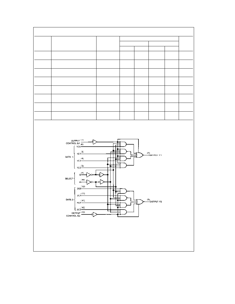
Logic Diagram
TL F 6416 ≠ 2
3

Physical Dimensions
inches (millimeters)
Ceramic Leadless Chip Carrier Package (E)
Order Number 54LS253LMQB
NS Package Number E20A
16-Lead Ceramic Dual-In-Line Package (J)
Order Number 54LS253DMQB or DM54LS253J
NS Package Number J16A
4
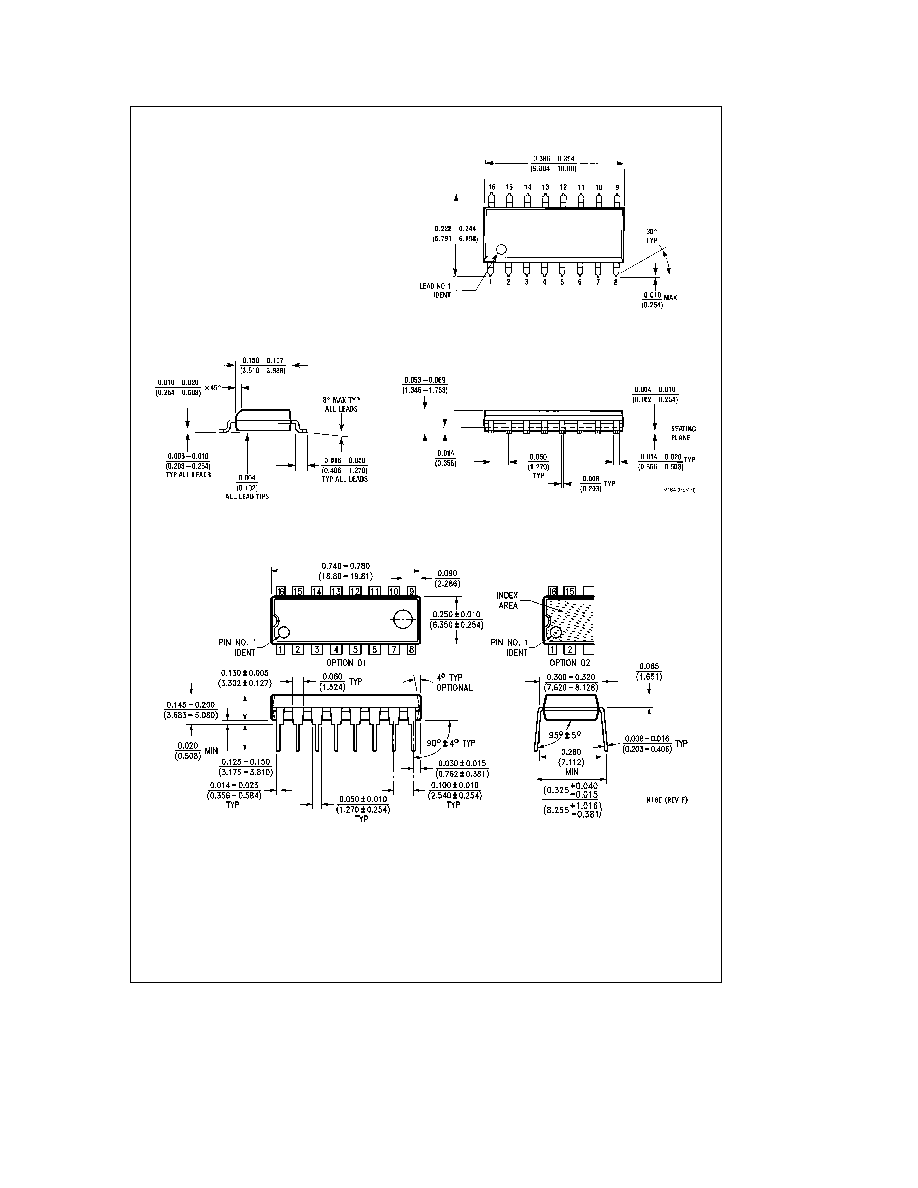
Physical Dimensions
inches (millimeters) (Continued)
16-Lead Small Outline Molded Package (M)
Order Number DM74LS253M
NS Package Number M16A
16-Lead Molded Dual-In-Line Package (N)
Order Number DM74LS253N
NS Package Number N16E
5