
TL F 9823
54LS256DM74LS256
Dual
4-Bit
Addressable
Latch
June 1989
54LS256 DM74LS256
Dual 4-Bit Addressable Latch
General Description
The 'LS256 is a dual 4-bit addressable latch with common
control inputs these include two Address inputs (A0 A1)
an active LOW enable input (E) and an active LOW Clear
input (CL) Each latch has a Data input (D) and four outputs
(Q0 ≠ Q3)
When the Enable (E) is HIGH and the Clear input (CL) is
LOW all outputs (Q0 ≠ Q3) are LOW Dual 4-channel demul-
tiplexing occurs when the CL and E are both LOW When
CL is HIGH and E is LOW the selected output (Q0 ≠ Q3)
determined by the Address inputs follows D When the E
goes HIGH the contents of the latch are stored When op-
erating in the addressable latch mode (E
e
LOW CL
e
HIGH) changing more than one bit of the Address (A0 A1)
could impose a transient wrong address Therefore this
should be done only while in the memory mode (E
e
CL
e
HIGH)
Features
Y
Serial-to-parallel capability
Y
Output from each storage bit available
Y
Random (addressable) data entry
Y
Easily expandable
Y
Active low common clear
Connection Diagram
Dual-In-Line Package
TL F 9823 ≠ 1
Order Number 54LS256DMQB
54LS256FMQB or DM74LS256N
See NS Package Number J16A
N16E or W16A
Logic Symbol
TL F 9823 ≠ 2
V
CC
e
Pin 16
GND
e
Pin 8
Pin Names
Description
A0 A1
Common Address Inputs
D
a
D
b
Data Inputs
E
Common Enable Input (Active LOW)
CL
Conditional Clear Input (Active LOW)
Q0
a
≠ Q
3
a
Side A Latch Outputs
Q0
b
≠ Q
3
b
Side B Latch Outputs
C1995 National Semiconductor Corporation
RRD-B30M115 Printed in U S A
Absolute Maximum Ratings
(Note)
If Military Aerospace specified devices are required
please contact the National Semiconductor Sales
Office Distributors for availability and specifications
Supply Voltage
7V
Input Voltage
7V
Operating Free Air Temperature Range
54LS
b
55 C to
a
125 C
DM74LS
0 C to
a
70 C
Storage Temperature Range
b
65 C to
a
150 C
Note
The ``Absolute Maximum Ratings'' are those values
beyond which the safety of the device cannot be guaran-
teed The device should not be operated at these limits The
parametric values defined in the ``Electrical Characteristics''
table are not guaranteed at the absolute maximum ratings
The ``Recommended Operating Conditions'' table will define
the conditions for actual device operation
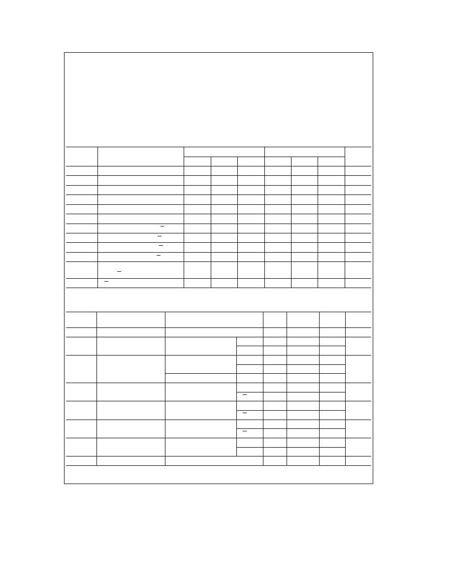
Recommended Operating Conditions
Symbol
Parameter
54LS256
DM74LS256
Units
Min
Nom
Max
Min
Nom
Max
V
CC
Supply Voltage
4 5
5
5 5
4 75
5
5 25
V
V
IH
High Level Input Voltage
2
2
V
V
IL
Low Level Input Voltage
0 7
0 8
V
I
OH
High Level Output Current
b
0 4
b
0 4
mA
I
OL
Low Level Output Current
4
8
mA
T
A
Free Air Operating Temperature
b
55
125
0
70
C
t
s
(H)
Setup Time HIGH D
n
to E
20
20
ns
t
h
(H)
Hold Time HIGH D
n
to E
0
0
ns
t
s
(L)
Setup Time LOW D
n
to E
15
15
ns
t
h
(L)
Hold Time LOW D
n
to E
0
0
ns
t
s
(H)
Setup Time HIGH or LOW
0
0
ns
t
s
(L)
A
n
to E
t
w
(L)
E Pulse Width LOW
17
17
ns
Electrical Characteristics
Over recommended operating free air temperature range (unless otherwise noted)
Symbol
Parameter
Conditions
Min
Typ
Max
Units
(Note 1)
V
I
Input Clamp Voltage
V
CC
e
Min I
I
e b
18 mA
b
1 5
V
V
OH
High Level Output
V
CC
e
Min I
OH
e
Max
54LS
2 5
V
Voltage
V
IL
e
Max
DM74
2 7
3 4
V
OL
Low Level Output
V
CC
e
Min I
OL
e
Max
54LS
0 4
Voltage
V
IH
e
Min
DM74
0 35
0 5
V
I
OL
e
4 mA V
CC
e
Min
DM74
0 25
0 4
I
I
Input Current
Max
V
CC
e
Max V
I
e
10V
Inputs
0 1
mA
Input Voltage
E
0 2
I
IH
High Level Input Current
V
CC
e
Max V
I
e
2 7V
Inputs
20
m
A
E
40
I
IL
Low Level Input Current
V
CC
e
Max V
I
e
0 4V
Inputs
b
0 4
mA
E
b
0 8
I
OS
Short Circuit
V
CC
e
Max
54LS
b
20
b
100
mA
Output Current
(Note 2)
DM74
b
20
b
100
I
CC
Supply Current
V
CC
e
Max
25
mA
Note 1
All typicals are at V
CC
e
5V T
A
e
25 C
Note 2
Not more than one output should be shorted at a time and the duration should not exceed one second
3


