
DS9622
Dual Line Receiver
General Description
The DS9622 is a dual line receiver designed to discriminate
a worst case logic swing of 2V from a
Ī
10V common mode
noise signal or ground shift. A 1.5V threshold is built into the
differential amplifier to offer a TTL compatible threshold volt-
age and maximum noise immunity. The offset is obtained by
use of current sources and matched resistors.
The DS9622 allows the choice of output states with the input
open, without affecting circuit performance by use of S3. A
130
terminating resistor is provided at the input of each line
receiver. An enable is also provided for each line receiver.
The output is TTL compatible. The output high level can be
increased to 12V by tying it to a positive supply through a re-
sistor. The output circuits allow wired-OR operation.
Features
n
TTL compatible threshold voltage
n
Input terminating resistors
n
Choice of output state with inputs open
n
TTL compatible output
n
High common mode
n
Wired-OR capability
n
Enable inputs
n
Logic compatible supply voltages
Connection Diagram
14≠Lead DIP
DS009760-2
Top View
For Complete Military 883 Specifications, see RETS Datasheet.
Order Number DS9622ME/883,
DS9622MJ/883 or DS9622MW/883
See NS Package Number E20A, J14A or W14B
October 1993
DS9622
Dual
Line
Receiver
© 1999 National Semiconductor Corporation
DS009760
www.national.com

Absolute Maximum Ratings
(Note 1)
If Military/Aerospace specified devices are required,
please contact the National Semiconductor Sales Office/
Distributors for availability and specifications.
Storage Temperature Range
-65įC to +175įC
Operating Temperature Range
-55įC to +125įC
Lead Temperature
(Soldering, 60 sec.)
300įC
Internal Power Dissipation (Note 5)
400 mW
V
+
to GND
-0.5V to +7.0V
Input Voltage
Ī
15V
Voltage Applied to Outputs
for Output High State
-0.5V to +13.2V
V
-
to GND
-0.5V to -12V
Enable to GND
-0.5V to +15V
Operating Conditions
Min
Max
Units
Supply Voltage, V
CC
4.5
5.5
V
Temperature, T
A
-55
+125
įC
Electrical Characteristics
(Notes 2, 3)
Symbol
Parameter
Conditions
Min
Max
Units
V
OL
Output Voltage LOW
V
+
= S3 = 4.5V, V
-
= -11V,
V
DIFF
= 2.0V, I
OL
= 12.4 mA,
0.4
V
EN = Open
V
OH
Output Voltage HIGH
V
+
= 4.5V, V
-
= -9.0V,
S3 = 0V, V
DIFF
= 1.0V,
2.8
V
I
OH
= -0.2 mA, EN = Open
I
CEX
Output Leakage Current
V
+
= 4.5V, V
-
= -11V,
S3 = 0V, V
DIFF
= 1.0V,
200
ĶA
V
O
= 12V, EN = Open
I
OS
Output Short Circuit
V
+
= 5.0V, V
-
= -10V,
Current (Note 4)
V
DIFF
= 1.0V, V
O
= S3 = 0V,
-3.1
-1.4
mA
EN = Open
I
R
(EN)
Enable Input
V
+
= S3 = 4.5V, V
-
= -11V,
5.0
ĶA
Leakage Current
I
N
= Open, EN = 4.0V
I
F
(EN)
Enable Input
V
+
= 5.5V, V
-
= -9.0V
-1.5
mA
Forward Current
V
I
= Open, EN = S3 = 0V
I
F
(+IN)
+Input Forward Current
V
+
= 5.0V, V
-
= -10V,
V
I
+
= 0V, V
I
-
= GND,
-2.3
mA
EN = S3 = Open
I
F
(-IN)
-Input Forward Current
V
+
= S3 = 5.0V, V
-
= -10V,
V
I
+
= GND, V
I
-
= 0V,
-2.6
mA
EN = Open
V
IL
(EN)
Input Voltage LOW
4.5V
V
+
5.5V,
+25įC
1.0
V
-11V
V
-
-9.0V,
+125įC
0.7
V
EN = Open
-55įC
1.3
V
V
TH
Differential Input
4.5V,
V
+
5.5V,
Threshold Voltage
-11V
V
-
-9.0V,
1.0
2.0
V
EN = Open
V
CM
Common Mode Voltage
V
+
= 5.0V, V
-
= -10V,
25įC
-10
+10
V
1.0V
V
DIFF
2.0V
R
T
Terminating Resistance
25įC
91
215
I
+
Positive Supply Current
V
+
= S3 = V
I
+
= 5.5V,
25įC
22.9
mA
I
-
Negative Supply Current
V
-
= 11V, V
I
-
= 0V
-11.1
mA
www.national.com
2

Electrical Characteristics
(Notes 2, 3) (Continued)
Symbol
Parameter
Conditions
Min
Max
Units
SWITCHING CHARACTERISTICS T
A
= 25įC
t
PLH
Propagation Delay
V
+
= 5.0V,
V
-
= -10V,
0V
V
I
3.0V,
C
L
= 30 pF
(See
Figure 1)
R
L
= 3.9 k
50
ns
to High Level
t
PHL
Propagation Delay
R
L
= 390
to Low Level
50
ns
Note 1: "Absolute Maximum Ratings" are those values beyond which the safety of the device cannot be guaranteed. They are not meant to imply that the devices
should be operated at these limits. The tables of "Electrical Characteristics" provide conditions for actual device operation.
Note 2: Unless otherwise specified Min/Max limits apply across the -55įC to +125įC temperature range. All typicals are given for V
CC
= 5V and T
A
= 25įC.
Note 3: All currents into device pins are positive; all currents out of device pins are negative. All voltages are referenced to ground unless otherwise specified.
Note 4: Only one output at a time should be shorted.
Note 5: Rating applies to ambient temperatures up to +125įC. Above 125įC ambient, derate linearity at 120įC/W.
Switching Time Test Circuit and Waveforms
Equivalent Circuit
DS009760-4
DS009760-5
FIGURE 1.
DS009760-6
www.national.com
3

Typical Applications
When S3 is connected to V-, open inputs cause output to be high. When V+ = 5V, V- = -10V and S3 is connected to ground,
open inputs cause output to be low.
www.national.com
4
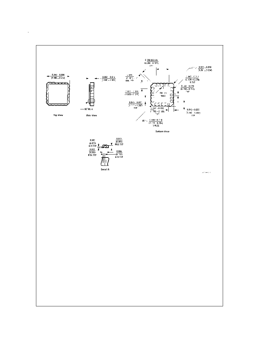
Physical Dimensions
inches (millimeters) unless otherwise noted
Ceramic Leadless Chip Carrier (LCC)
Order Number DS9622ME/883
NS Package Number E20A
www.national.com
5