
54FCT245
Octal Bidirectional Transceiver with TRI-STATE
Æ
Outputs
General Description
The 'FCT245 contains eight non-inverting bidirectional buff-
ers with TRI-STATE outputs and is intended for bus-oriented
applications. Current sinking capability is 48 mA on both the
A and B ports. The Transmit/Receive (T/R) input determines
the direction of data flow through the bidirectional trans-
ceiver. Transmit (active HIGH) enables data from A ports to B
ports; Receive (active LOW) enables data from B ports to A
ports. The Output Enable input, when HIGH, disables both A
and B ports by placing them in a High Z condition.
Features
n
TTL input and output level compatible
n
A and B output sink capability of 48 mA, source
capability of 12 mA
n
CMOS power consumption
n
Standard Microcircuit Drawing (SMD) 5962-8762901
Ordering Code:
Military
Package
Package Description
Number
54FCT245DMQB
J20A
20-Lead Ceramic Dual-In-Line
54FCT245FMQB
W20A
20-Lead Cerpak
54FCT245LMQB
E20A
20-Lead Ceramic Leadless Chip Carrier, Type C
Logic Symbol
TRI-STATE
Æ
is a registered trademark of National Semiconductor Corporation.
DS100950-1
August 1998
54FCT245
Octal
Bidirectional
T
ransceiver
with
TRI-ST
A
T
E
Outputs
© 1998 National Semiconductor Corporation
DS100950
www.national.com
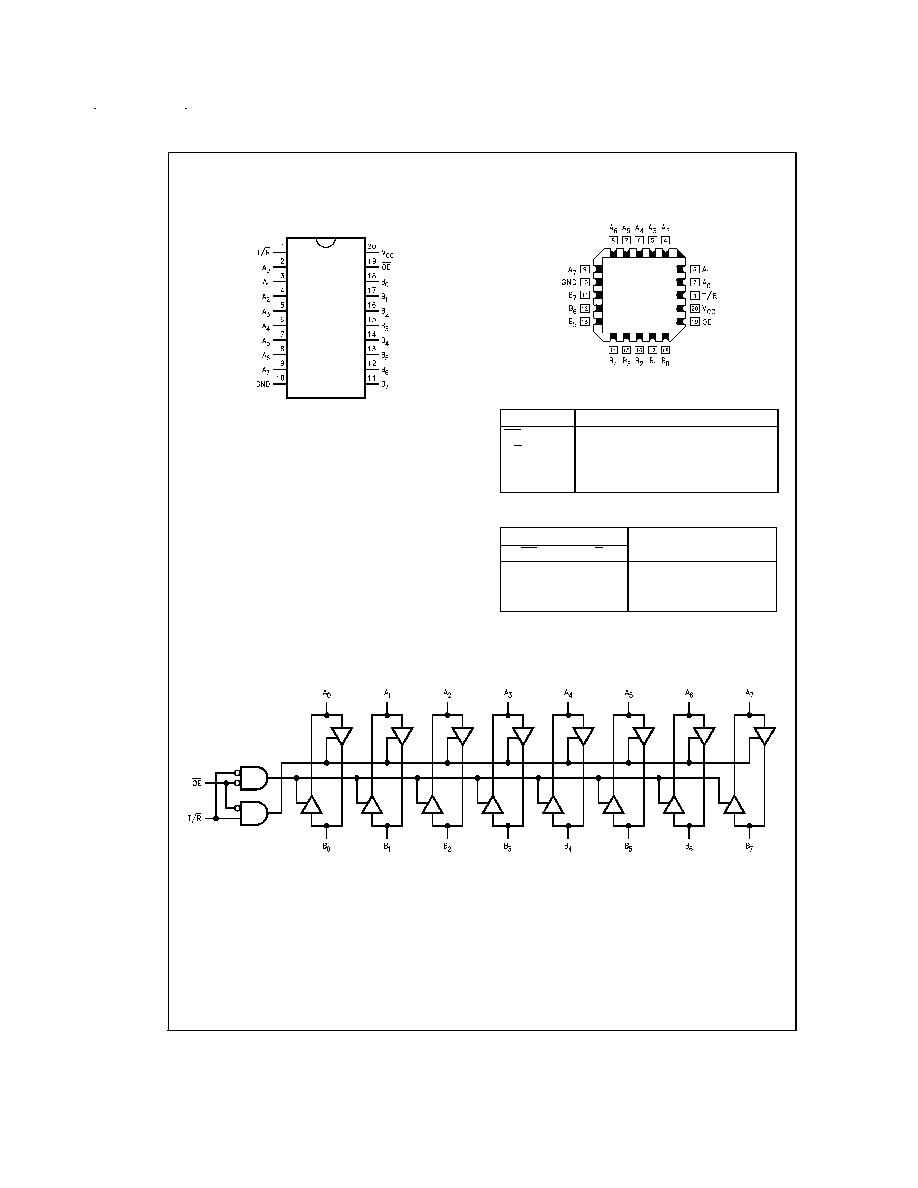
Connection Diagrams
Pin Descriptions
Pin Names
Description
OE
Output Enable Input (Active LOW)
T/R
Transmit/Receive Input
A
0
≠A
7
Side A Inputs or TRI-STATE Outputs
B
0
≠B
7
Side B Inputs or TRI-STATE Outputs
Truth Table
Inputs
Output
OE
T/R
L
L
Bus B Data to Bus A
L
H
Bus A Data to Bus B
H
X
High Z State
H = HIGH Voltage Level
L = LOW Voltage Level
X = Immaterial
Logic Diagram
Pin Assignment for DIP
and Flatpak.
DS100950-5
Pin Assignment for LCC
DS100950-3
DS100950-4
www.national.com
2

Absolute Maximum Ratings
(Note 1)
If Military/Aerospace specified devices are required,
please contact the National Semiconductor Sales Office/
Distributors for availability and specifications.
Storage Temperature
-65∞C to +150∞C
Ambient Temperature under Bias
-55∞C to +125∞C
Junction Temperature under Bias
Ceramic
-55∞C to +175∞C
V
CC
Pin Potential to
Ground Pin
-0.5V to +7.0V
Input Voltage (Note 2)
-0.5V to +7.0V
Input Current (Note 2)
-30 mA to +5.0 mA
Voltage Applied to Any Output
in the Disabled or
Power-off State
-0.5V to 5.5V
in the HIGH State
-0.5V to V
CC
Current Applied to Output
in LOW State (Max)
twice the rated I
OL
(mA)
Recommended Operating
Conditions
Free Air Ambient Temperature
Military
-55∞C to +125∞C
Supply Voltage
Military
+4.5V to +5.5V
Note 1: Absolute maximum ratings are values beyond which the device may
be damaged or have its useful life impaired. Functional operation under these
conditions is not implied.
Note 2: Either voltage limit or current limit is sufficient to protect inputs.
DC Electrical Characteristics
Symbol
Parameter
FCT245
Units
V
CC
Conditions
Min
Max
V
IH
Input HIGH Voltage
2.0
V
Recognized HIGH Signal
V
IL
Input LOW Voltage
0.8
V
Recognized LOW Signal
V
CD
Input Clamp Diode Voltage
-1.2
V
Min
I
IN
= -18 mA (OE, T/R)
V
OH
Output HIGH
Voltage
54FCT
4.3
V
Min
I
OH
= -300 uA (A
n
, B
n
)
54FCT
2.4
V
Min
I
OH
= -12 mA (A
n
, B
n
)
V
OL
Output LOW
Voltage
54FCT
0.2
V
Min
I
OL
= 300 uA (A
n
, B
n
)
54FCT
0.55
V
Min
I
OL
= 48 mA (A
n
, B
n
)
I
IH
Input HIGH Current
5
µA
Max
V
IN
= 2.7V (OE, T/R)
5
V
IN
= V
CC
(OE, T/R)
I
BVIT
Input HIGH Current Breakdown Test
(I/O)
20
µA
Max
V
IN
= 5.5V (A
n
, B
n
)
I
IL
Input LOW Current
-5
µA
Max
V
IN
= 0.0V (OE, T/R)
I
OS
Output Short-Circuit Current
-60
mA
Max
V
OUT
= 0.0V (A
n
, B
n
)
I
CCQ
Power Supply Current
1.5
mA
Max
V
IN
= 0.2V or V
IN
= 5.3V, V
CC
=
5.5V
I
CC
Power Supply Current
2.0
mA
Max
V
CC
= 5.5V, V
IN
= 3.4V
I
CCT
Total Power Supply Current
6.0
mA
V
IN
= 3.4V or V
IN
= GND, OE =
T/R = GND, V
CC
= 5.5V, f
I
=
10Mhz, outputs open, one bit
toggling - 50% duty cycle
5.5
mA
Max
V
IN
= 5.3V or V
IN
= 0.2V,OE =
T/R = GND, V
CC
= 5.5V, f
I
=
10Mhz, outputs open, one bit
toggling - 50% duty cycle
I
CCD
Dynamic I
CC
(Note 3)
0.4
mA/
MHz
Max
Outputs Open, OE =GND, T/R =
GND or V
CC
One Bit Toggling,
50% Duty Cycle
Note 3: Guaranteed but not tested.
www.national.com
3

AC Electrical Characteristics
Symbol
Parameter
54FCT
Units
Fig.
No.
T
A
= -55∞C to +125∞C
V
CC
= 4.5V≠5.5V
C
L
= 50 pF
Min
Max
t
PLH
Propagation Delay
1.5
7.5
ns
Figure
4
t
PHL
Data to Outputs
1.5
7.5
t
PZH
Output Enable
1.5
10.0
ns
Figure
5
t
PZL
Time
1.5
10.0
t
PHZ
Output Disable
1.5
10.0
ns
Figure
5
t
PLZ
Time
1.5
10.0
Capacitance
Symbol
Parameter
Max
Units
Conditions
T
A
= 25∞C
C
IN
Input Capacitance
10.0
pF
V
CC
= 0V (OE , T/R)
C
I/O
(Note 4)
I/O Capacitance
12.0
pF
V
CC
= 5.0V (A
n
, B
n
)
Note 4: C
I/O
is measured at frequency f = 1 MHz, per MIL-STD-883B, Method 3012.
AC Loading
DS100950-6
*
Includes jig and probe capacitance
FIGURE 1. Standard AC Test Load
DS100950-7
FIGURE 2. Test Input Signal Levels
Amplitude
Rep. Rate
t
w
t
r
t
f
3.0V
1 MHz
500 ns
2.5 ns
2.5 ns
FIGURE 3. Test Input Signal Requirements
www.national.com
4

AC Waveforms
DS100950-8
FIGURE 4. Propagation Delay Waveforms
for Inverting and Non-Inverting Functions
DS100950-10
FIGURE 5. TRI-STATE Output HIGH
and LOW Enable and Disable Times
www.national.com
5