54ACT563
Octal Latch with TRI-STATE
Æ
Outputs
General Description
The 'ACT563 is a high-speed octal latch with buffered com-
mon Latch Enable (LE) and buffered common Output Enable
(OE) inputs.
The 'ACT563 device is functionally identical to the 'ACT573,
but with inverted outputs.
Features
n
I
CC
and I
OZ
reduced by 50%
n
Inputs and outputs on opposite sides of package allow
easy interface with microprocessors
n
Useful as input or output port for microprocessors
n
Functionally identical to 'ACT573 but with inverted
outputs
n
Outputs source/sink 24 mA
n
'ACT563 has TTL-compatible inputs
n
Standard Military Drawing (SMD)
-- 'ACT563: 5962-89556
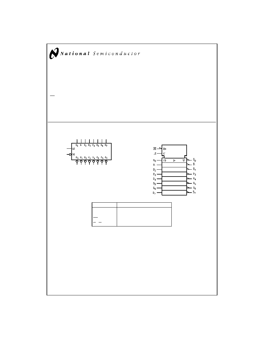
Logic Symbols
Pin Names
Description
D
0
≠D
7
Data Inputs
LE
Latch Enable Input
OE
TRI-STATE Output Enable Input
O
0
≠O
7
TRI-STATE Latch Outputs
TRI-STATE
Æ
is a registered trademark of National Semiconductor Corporation.
FACT
TM
is a trademark of Fairchild Semiconductor Corporation.
DS100331-1
IEEE/IEC
DS100331-2
July 1998
54ACT563
Octal
Latch
with
TRI-ST
A
T
E
Outputs
© 1998 National Semiconductor Corporation
DS100331
www.national.com
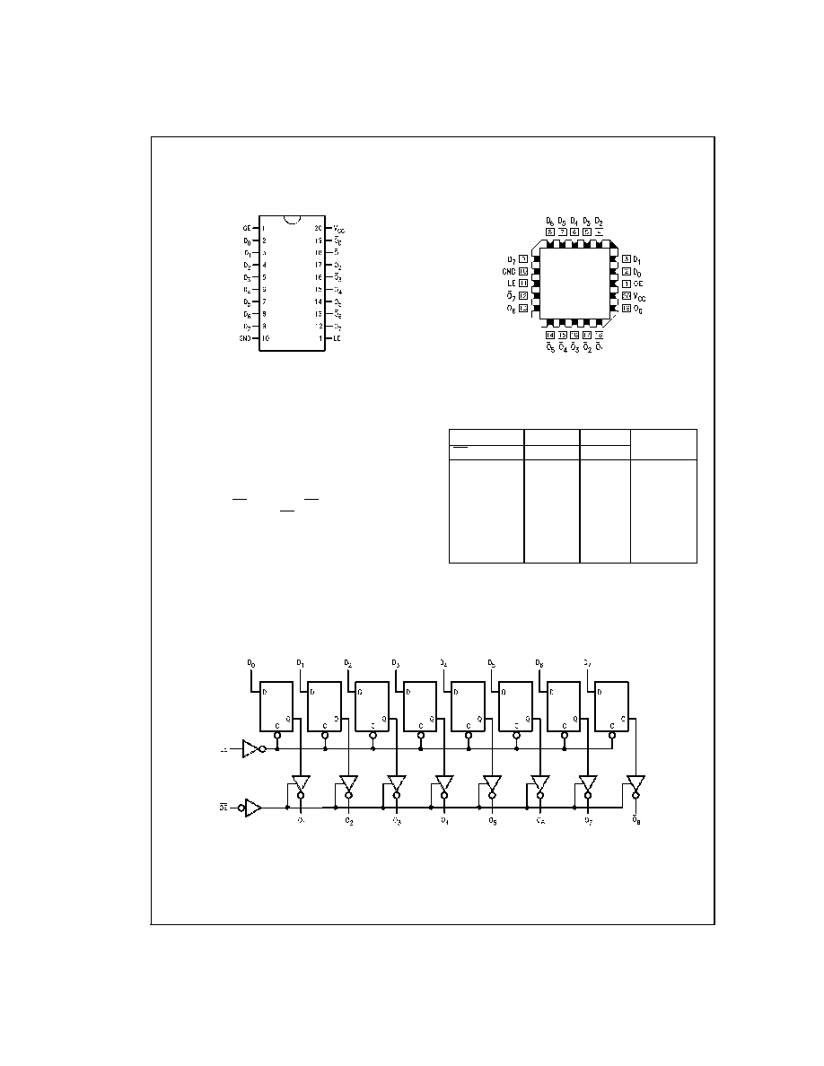
Connection Diagrams
Functional Description
The 'ACT563 contains eight D-type latches with TRI-STATE
complementary outputs. When the Latch Enable (LE) input
is HIGH, data on the D
n
inputs enters the latches. In this con-
dition the latches are transparent, i.e., a latch output will
change state each time its D input changes. When LE is
LOW the latches store the information that was present on
the D inputs a setup time preceding the HIGH-to-LOW tran-
sition of LE. The TRI-STATE buffers are controlled by the
Output Enable (OE) input. When OE is LOW, the buffers are
in the bi-state mode. When OE is HIGH the buffers are in the
high impedance mode but that does not interfere with enter-
ing new data into the latches.
Function Table
Inputs
Internal
Outputs
Function
OE
LE
D
Q
O
H
X
X
X
Z
High-Z
H
H
L
H
Z
High-Z
H
H
H
L
Z
High-Z
H
L
X
NC
Z
Latched
L
H
L
H
H
Transparent
L
H
H
L
L
Transparent
L
L
X
NC
NC
Latched
H = HIGH Voltage Level
L = LOW Voltage Level
X = Immaterial
Z = High Impedance
NC = No Change
Logic Diagram
Pin Assignment
for DIP and Flatpak
DS100331-3
Pin Assignment
for LCC
DS100331-4
DS100331-5
Please note that this diagram is provided only for the understanding of logic operations and should not be used to estimate propagation delays.
www.national.com
2

Absolute Maximum Ratings
(Note 1)
If Military/Aerospace specified devices are required,
please contact the National Semiconductor Sales Office/
Distributors for availability and specifications.
Supply Voltage (V
CC
)
-0.5V to +7.0V
DC Input Diode Current (I
IK
)
V
I
= -0.5V
-20 mA
V
I
= V
CC
+ 0.5V
+20 mA
DC Input Voltage (V
I
)
-0.5V to V
CC
+ 0.5V
DC Output Diode Current (I
OK
)
V
O
= -0.5V
-20 mA
V
O
= V
CC
+ 0.5V
+20 mA
DC Output Voltage (V
O
)
-0.5V to V
CC
+ 0.5V
DC Output Source
or Sink Current (I
O
)
±
50 mA
DC V
CC
or Ground Current
per Output Pin (I
CC
or I
GND
)
±
50 mA
Storage Temperature (T
STG
)
-65∞C to +150∞C
Junction Temperature (T
J
)
CDIP
175∞C
Recommended Operating
Conditions
Supply Voltage (V
CC
)
'ACT
4.5V to 5.5V
Input Voltage (V
I
)
0V to V
CC
Output Voltage (V
O
)
0V to V
CC
Operating Temperature (T
A
)
54ACT
-55∞C to +125∞C
Minimum Input Edge Rate (
V/
t)
'ACT Devices
V
IN
from 0.8V to 2.0V
V
CC
@
4.5V, 5.5V
125 mV/ns
Note 1: Absolute maximum ratings are those values beyond which damage
to the device may occur. The databook specifications should be met, without
exception, to ensure that the system design is reliable over its power supply,
temperature, and output/input loading variables. National does not recom-
mend operation of FACT
TM
circuits outside databook specifications.
DC Characteristics for 'ACT Family Devices
54ACT
Symbol
Parameter
V
CC
T
A
=
Units
Conditions
(V)
-55∞C to +125∞C
Guaranteed Limits
V
IH
Minimum High Level
4.5
2.0
V
V
OUT
= 0.1V
Input Voltage
5.5
2.0
or V
CC
- 0.1V
V
IL
Maximum Low Level
4.5
0.8
V
V
OUT
= 0.1V
Input Voltage
5.5
0.8
or V
CC
- 0.1V
V
OH
Minimum High Level
4.5
4.4
V
I
OUT
= -50 µA
Output Voltage
5.5
5.4
(Note 2)
V
IN
= V
IL
or V
IH
4.5
3.70
V
I
OH
= -24 mA
5.5
4.70
I
OH
= -24 mA
V
OL
Maximum Low Level
4.5
0.1
V
I
OUT
= 50 µA
Output Voltage
5.5
0.1
(Note 2)
V
IN
= V
IL
or V
IH
4.5
0.50
V
I
OL
= 24 mA
5.5
0.50
I
OL
= 24 mA
I
IN
Maximum Input
5.5
±
1.0
µA
V
I
= V
CC
, GND
Leakage Current
I
OZ
Maximum TRI-STATE
5.5
±
5.0
µA
V
I
= V
IL
, V
IH
Current
V
O
= V
CC
, GND
I
CCT
Maximum I
CC
/Input
5.5
1.6
mA
V
I
= V
CC
- 2.1V
(Note 3)
I
OLD
Minimum Dynamic
5.5
50
mA
V
OLD
= 1.65V Max
I
OHD
Output Current
5.5
-50
mA
V
OHD
= 3.85V Min
I
CC
Maximum Quiescent
5.5
80.0
µA
V
IN
= V
CC
Supply Current
or GND
Note 2: All outputs loaded; thresholds on input associated with output under test.
Note 3: Maximum test duration 2.0 ms, one output loaded at a time.
Note 4: I
CC
for 54ACT
@
25∞C is identical to 74ACT
@
25∞C.
3
www.national.com

AC Electrical Characteristics
54ACT
V
CC
T
A
= -55∞C
Fig.
Symbol
Parameter
(V)
to +125∞C
Units
No.
(Note 5)
C
L
= 50 pF
Min
Max
t
PLH
Propagation Delay
5.0
1.0
14.5
ns
D
n
to O
n
t
PHL
Propagation Delay
5.0
1.0
12.0
ns
D
n
to O
n
t
PLH
Propagation Delay
5.0
1.0
12.5
ns
LE to O
n
t
PHL
Propagation Delay
5.0
1.0
11.5
ns
LE to O
n
t
PZH
Output Enable Time
5.0
1.0
11.5
ns
t
PZL
Output Enable Time
5.0
1.0
11.0
ns
t
PHZ
Output Disable Time
5.0
1.0
12.0
ns
t
PLZ
Output Disable Time
5.0
1.0
9.5
ns
Note 5: Voltage Range 5.0 is 5.0V
±
0.5V
AC Operating Requirements
54ACT
V
CC
T
A
= -55∞C
Fig.
Symbol
Parameter
(V)
to +125∞C
Units
No.
(Note 6)
C
L
= 50 pF
Guaranteed Minimum
t
s
Setup Time, HIGH or LOW
5.0
4.5
ns
D
n
to LE
t
h
Hold Time, HIGH or LOW
5.0
1.5
ns
D
n
to LE
t
w
LE Pulse Width, HIGH
5.0
5.0
ns
Note 6: Voltage Range 5.0 is 5.0V
±
0.5V
Capacitance
Symbol
Parameter
Typ
Units
Conditions
C
IN
Input Capacitance
4.5
pF
V
CC
= OPEN
C
PD
Power Dissipation
50.0
pF
V
CC
= 5.0V
Capacitance
www.national.com
4

Physical Dimensions
inches (millimeters) unless otherwise noted
20 Terminal Ceramic Leadless Chip Carrier (L)
NS Package Number E20A
20-Lead Ceramic Dual-In-Line Package (D)
NS Package Number J20A
5
www.national.com