
DS96F172M/DS96F174C/DS96F174M
EIA-485/EIA-422 Quad Differential Drivers
General Description
The DS96F172 and the DS96F174 are high speed quad dif-
ferential line drivers designed to meet EIA-485 Standards.
The DS96F172 and the DS96F174 offer improved perfor-
mance due to the use of L-FAST bipolar technology. The use
of LFAST technology allows the DS96F172 and DS96F174
to operate at higher speeds while minimizing power con-
sumption.
The DS96F172 and the DS96F174 have TRI-STATE
Æ
out-
puts and are optimized for balanced multipoint data bus
transmission at rates up to 15 Mbps. The drivers have wide
positive and negative common mode range for multipoint ap-
plications in noisy environments. Positive and negative
current-limiting is provided which protects the drivers from
line fault conditions over a +12V to -7.0V common mode
range. A thermal shutdown feature is also provided. The
DS96F172 features an active high and active low Enable,
common to all four drivers. The DS96F174 features separate
active high Enables for each driver pair.
Features
n
Meets EIA-485 and EIA-422 standards
n
Monotonic differential output switching
n
TRI-STATE outputs
n
Designed for multipoint bus transmission
n
Common mode output voltage range: -7.0V to +12V
n
Operates from single +5.0V supply
n
Reduced power consumption
n
Thermal shutdown protection
n
DS96F172 and DS96F174 are lead and function
compatible with the SN75172/174 or the
AM26LS31/MC3487
n
Military temperature range available
n
Qualified for MIL-STD-883C
n
Standard military drawings available (SMD)
n
Available in DIP (J), LCC (E), and Flatpak (W) packages
Logic Diagrams
Function Tables
(Each Driver)
DS96F172
Input
Enable
Outputs
A
E
E
Y
Z
H
H
X
H
L
L
H
X
L
H
H
X
L
H
L
L
X
L
L
H
X
L
H
Z
Z
DS96F174
Input
Enable
Outputs
A
E
Y
Z
H
H
H
L
L
H
L
H
X
L
Z
Z
H = High Level
L = Low Level
X = Don't Care
Z = High Impedance (Off)
TRI-STATE
Æ
is a registered trademark of National Semiconductor Corporation.
DS96F172
DS009625-14
DS96F174
DS009625-15
July 2000
DS96F172M/DS96F174C/DS96F174M
EIA-485/EIA-422
Quad
Differential
Drivers
© 2000 National Semiconductor Corporation
DS009625
www.national.com
COMMERCIAL
Absolute Maximum Ratings
(Note 2)
Specifications for the 883 version of this product are
listed separately on the following pages.
Storage Temperature Range (T
STG
)
-65∞C to +175∞C
Lead Temperature (Soldering, 60 sec.)
300∞C
Maximum Package Power Dissipation (Note 1) at 25∞C
Ceramic DIP (J)
1500 mW
Supply Voltage
7.0V
Enable Input Voltage
5.5V
Recommended Operating
Conditions
Min
Typ
Max
Units
Supply Voltage (V
CC
)
DS96F174C
4.75
5.0
5.25
V
Common Mode
-7.0
+12.0
V
Output Voltage (V
OC
)
Output Current HIGH (I
OH
)
-60
mA
Output Current LOW (I
OL
)
60
mA
Operating Temperature
(T
A
)
DS96F174C
0
+70
∞C
Note 1: Derate "J" package 10 mW/∞C above 25∞C.
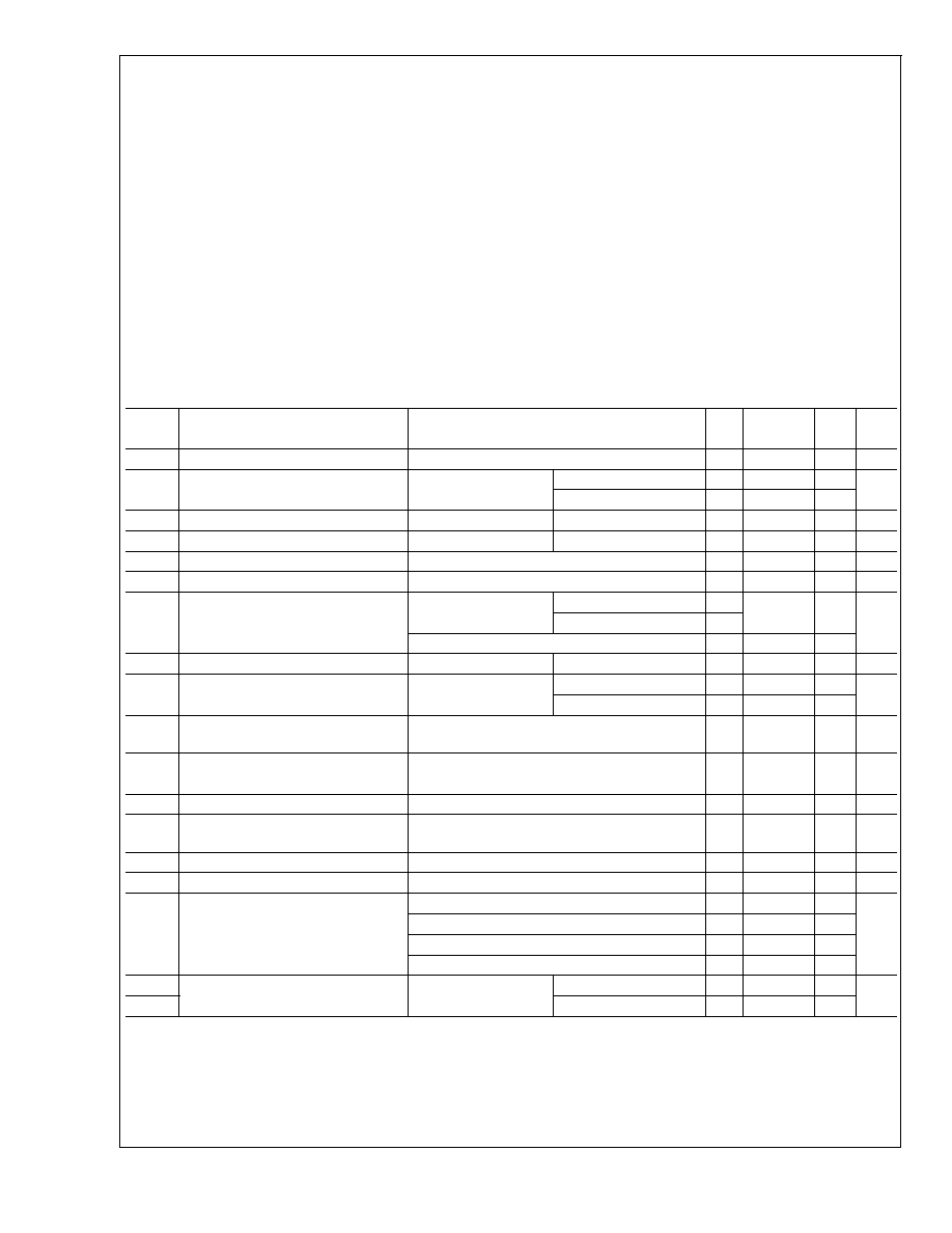
Electrical Characteristics
(Notes 3, 4)
Over recommended supply voltage and operating temperature range, unless otherwise specified
Symbol
Parameter
Conditions
Min
Typ
Max Units
(Note 2)
V
IH
Input Voltage HIGH
2.0
V
V
IL
Input Voltage LOW
T
A
= 0∞C to +70∞C
0.8
V
T
A
= -55∞C to +125∞C
0.7
V
OH
Output Voltage HIGH
I
OH
= -33 mA
T
A
= 0∞C to +70∞C
3.0
V
V
OL
Output Voltage LOW
I
OL
= 33 mA
T
A
= 0∞C to +70∞C
2.0
V
V
IC
Input Clamp Voltage
I
I
= -18 mA
-1.5
V
|V
OD1
|
Differential Output Voltage
I
O
= 0 mA
6.0
V
|V
OD2
|
Differential Output Voltage
R
L
= 54
,
Figure 1
T
A
= -55∞C
1.2
2.0
V
1.5
R
L
= 100
,
Figure 1
2.0
2.3
V
OD
Differential Output Voltage
Figure 2
T
A
= 0∞C to +70∞C
1.0
V
|V
OD
|
Change in Magnitude of Differential
R
L
= 54
or 100
,
-40∞C to +125∞C
±
0.2
V
Output Voltage (Note 5)
Figure 1
-55∞C to +125∞C
±
0.4
V
OC
Common Mode Output Voltage
(Note 6)
R
L
= 54
or 100
,
Figure 1
3.0
V
|V
OC
|
Change in Magnitude of Common
R
L
= 54
or 100
,
Figure 1
±
0.2
V
Mode Output Voltage (Note 5)
I
O
Output Current with Power Off
V
CC
= 0V, V
O
= -7.0V to +12V
±
50
µA
I
OZ
High Impedance State Output
Current
V
O
= -7.0V to +12V
±
20
±
50
µA
I
IH
Input Current HIGH
V
I
= 2.4V
20
µA
I
IL
Input Current LOW
V
I
= 0.4V
-50
µA
I
OS
Short Circuit Output Current
V
O
= -7.0V
-250
(Note 7)
V
O
= 0V
-150
mA
V
O
= V
CC
150
V
O
= +12V
250
I
CC
Supply Current (All Drivers)
No Load
Outputs Enabled
50
mA
I
CCX
Outputs Disabled
30
DS96F172M/DS96F174C/DS96F174M
www.national.com
2
COMMERCIAL
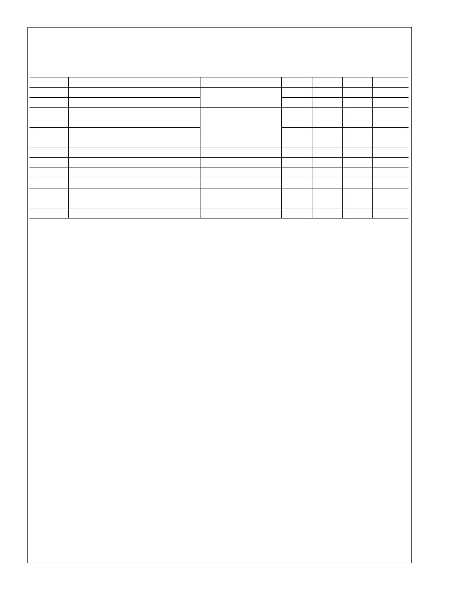
Switching Characteristics
V
CC
= 5.0V, T
A
= 25∞C
Symbol
Parameter
Conditions
Min
Typ
Max
Units
t
DD
Differential Output Delay Time
R
L
= 60
,
Figure 3
15
20
ns
t
TD
Differential Output Transition Time
15
22
ns
t
PLH
Propagation Delay Time,
R
L
= 27
,
Figure 4
12
16
ns
Low-to-High Level Output
t
PHL
Propagation Delay Time,
12
16
ns
High-to-Low Level Output
t
ZH
Output Enable Time to High Level
R
L
= 110
,
FIgure 4
25
32
ns
t
ZL
Output Enable Time to Low Level
R
L
= 110
,
Figure 6
25
32
ns
t
HZ
Output Disable Time from High Level
R
L
= 110
,
Figure 5
25
30
ns
t
LZ
Output Disable Time from Low Level
R
L
= 110
,
Figure 6
20
25
ns
t
LZL
Output Disable Time from Low Level
Figure 6
300
ns
with Load Resistor to GND (Note 8)
t
SKEW
Driver Output to Output
R
L
= 60
1.0
4.0
ns
Note 2: "Absolute Maximum Ratings" are those values beyond which the safety of the device cannot be guaranteed. They are not meant to imply that the devices
should be operated at these limits. The tables of "Electrical Characteristics" provide conditions for actual device operation.
Note 3: Unless otherwise specified min/max limits apply across the 0∞C to +70∞C range for the DS96F174C. All typicals are given for V
CC
= 5V and T
A
= 25∞C.
Note 4: All currents into the device pins are positive; all currents out of the device pins are negative. All voltages are reference to ground unless otherwise specified.
Note 5:
|V
OD
| and
|V
OC
| are the changes in magnitude of V
OD
and V
OC
respectively, that occur when the input is changed from a high level to a low level.
Note 6: In EIA-422A and EIA-485 standards, V
OC
, which is the average of the two output voltages with respect to ground, is called output offset voltage, V
OS
.
Note 7: Only one output at a time should be shorted.
Note 8: For more information see Application Bulletin, contact Product Marketing.
Order Number: DS96F174CJ
DS96F174CN
NS Package Number J16A or N16E
DS96F172M/DS96F174C/DS96F174M
www.national.com
3

MIL-STD-883C
Absolute Maximum Ratings
(Note 2)
For complete Military Specifications, refer to the appro-
priate SMD or MDS.
Storage Temperature Range (T
STG
)
-65∞C to +175∞C
Lead Temperature (Soldering, 60 sec.)
300∞C
Maximum Package Power Dissipation (Note 9) at 25∞C
Ceramic LCC (E)
2000 mW
Ceramic DIP (J)
1800 mW
Ceramic Flatpak (W)
1000 mW
Supply Voltage
7.0V
Enable Input Voltage
5.5V
Recommended Operating
Conditions
Min
Typ
Max
Units
Supply Voltage (V
CC
)
DS96F172M/DS96F174M
4.50
5.0
5.50
V
Common Mode
-7.0
+12.0
V
Output Voltage (V
OC
)
Output Current HIGH (I
OH
)
-60
mA
Output Current LOW (I
OL
)
60
mA
Operating Temperature (T
A
)
DS96F172M/DS96F174M
-55
+125
Note 9: Above T
A
= 25∞C, derate "E" package 13.4, "J" package 12.5, "W"
package 7.1 mW/∞C
Electrical Characteristics
(Notes 3, 4)
Over recommended supply voltage and operating temperature range unless otherwise specified
Symbol
Parameter
Conditions
Min
Max
Units
V
IH
Input Voltage HIGH
2.0
V
V
IL
Input Voltage LOW
T
A
= 25∞C
0.8
V
T
A
= -55∞C, or +125∞C
0.7
V
IC
Input Clamp Voltage
I
I
= -18 mA
-1.5
V
|V
OD1
|
Differential Output Voltage
I
O
= 0 mA
6.0
V
|V
OD2
|
Differential Output Voltage
R
L
= 54
, V
CC
= 4.5V
T
A
= -55∞C
1.2
Figure 1
T
A
= 25∞C, or +125∞C
1.5
V
R
L
= 100
, V
CC
= 4.5V,
Figure 1
2.0
|V
OD
|
Change in Magnitude of Differential
R
L
= 54
or 100
,
T
A
= 25∞C, or +125∞C
±
0.2
V
Output Voltage (Note 5)
V
CC
= 4.5V,
Figure 1
T
A
= -55∞C
±
0.4
V
V
OC
Common Mode Output Voltage
(Note 6)
R
L
= 54
or 100
,
Figure 1
3.0
V
|V
OC
|
Change in Magnitude of Common
R
L
= 54
or 100
, V
CC
= 4.5V,
Figure 1
±
0.2
V
Mode Output Voltage (Note 5)
I
O
Output Current with Power Off
V
CC
= 0V, V
O
= -7.0V to +12V
±
50
µA
I
OZ
High Impedance State Output Current
V
O
= -7.0V to +12V
±
50
µA
I
IH
Input Current HIGH
V
I
= 2.4V
20
µA
I
IL
Input Current LOW
V
I
= 0.4V
-50
µA
I
OS
Short Circuit Output Current
V
O
= -7.0V
-250
(Note 7)
V
O
= 0V
-150
mA
V
O
= V
CC
150
V
O
= +12V
250
I
CC
Supply Current (All Drivers)
No Load
Outputs Enabled
50
mA
I
CCX
Outputs Disabled
30
DS96F172M/DS96F174C/DS96F174M
www.national.com
4
MIL-STD-883C
Switching Characteristics
V
CC
= 5.0V
Symbol
Parameter
Conditions
T
A
= 25∞C
T
A
= 55∞C
T
A
= 125∞C
Units
Typ
Max
Max
Max
t
DD
Differential Output Delay Time
R
L
= 60
, C
L
= 15 pF,
15
22
30
30
ns
t
TD
Differential Output Transition Time
Figure 3
15
22
40
40
ns
t
PLH
Propagation Delay Time,
R
L
= 27
, C
L
= 15 pF,
12
16
25
25
ns
Low-to-High Level Output
Figure 4
t
PHL
Propagation Delay Time,
12
16
25
25
ns
High-to-Low Level Output
t
ZH
Output Enable Time to High Level
R
L
= 110
,
Figure 5
25
32
40
40
ns
t
ZL
Output Enable Time to Low Level
R
L
= 110
,
Figure 6
25
35
100
100
ns
t
HZ
Output Disable Time from High Level
R
L
= 110
,
Figure 5,
25
30
80
80
ns
Note 13
t
LZ
Output Disable Time from Low Level
R
L
= 110
,
Figure 6
20
25
40
40
ns
t
LZL
Output Disable Time from Low Level
Figure 6
300
ns
with Load Resistor to GND (Note 12)
t
SKEW
Driver Output to Output
R
L
= 60
1.0
4.0
10
10
ns
SMD Numbers: DS96F172MJ/883
5962-9076501MEA
DS96F174MJ/883
5962-9076502MEA
DS96F172ME/883
5962-9076501M2A
DS96F174MW/883
5962-9076502MFA
DS96F174ME/883
5962-9076502M2A
Order Number: DS96F172MJ/883, DS96F174MJ/883
NS Package Number J16A
DS96F172ME/883, DS96F174ME/883
NS Package Number E20A
DS96F172MW-MIL, DS96F174MW/883
NS Package Number W16A
For Complete Military Product Specifications, refer to the appropriate SMD or MDS.
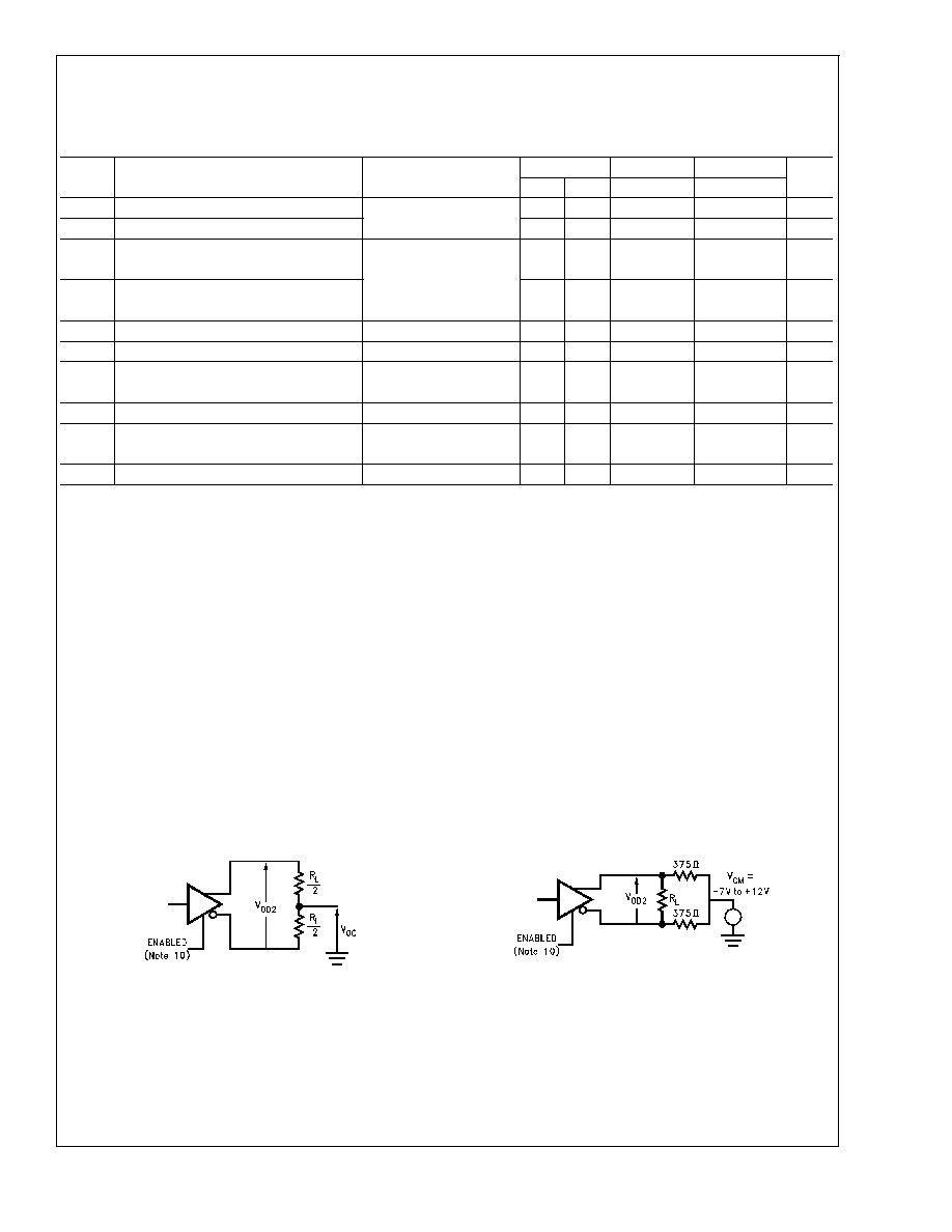
Parameter Measurement Information
DS009625-3
FIGURE 1. Differential and Common
Mode Output Voltage
DS009625-13
FIGURE 2. Differential Output Voltage with
Varying Common Mode Voltage
DS96F172M/DS96F174C/DS96F174M
www.national.com
5