
54ACT818
8-Bit Diagnostic Register
General Description
The 'ACT818 is a high-speed, general-purpose pipeline reg-
ister with an on-board diagnostic register for performing se-
rial diagnostics and/or writable control store loading.
The D-to-Y path provides an 8-bit parallel data path pipeline
register for normal system operation. The diagnostic register
can load parallel data to or from the pipeline register and can
output data through the D input port (as in WCS loading).
The 8-bit diagnostic register has multiplexer inputs that se-
lect parallel inputs from the Y-port or adjacent bits in the di-
agnostic register to operate as a right-shift-only register. This
register can then participate in a serial loop throughout the
system where normal data, address, status and control reg-
isters are replaced with 'ACT818 diagnostic pipeline regis-
ters. The loop can be used to scan in a complete test routine
starting point (Data, Address, etc.). Then after a specified
number of machine cycles it scans out the results to be in-
spected for the expected results. WCS loading can be ac-
complished using the same technique. An instruction word
can be serially shifted into the shadow register and written
into the WCS RAM by enabling the D output.
Features
n
On-line and off-line system diagnostics
n
Swaps the contents of diagnostic register and output
register
n
Diagnostic register and diagnostic testing
n
Cascadable for wide control words as used in
microprogramming
n
Edge-triggered D registers
n
Outputs source/sink 24 mA
n
'ACT818 has TTL-compatible inputs
n
'ACT818 is functionally- and pin-compatible to AMD
Am29818 and MMI 74S818
n
Standard Microcircuit Drawing (SMD) 5962-9160901
Applications
n
Register for microprogram control store
n
Status register
n
Data register
n
Instruction register
n
Interrupt mask register
n
Pipeline register
n
General purpose register
n
Parallel-serial/serial-parallel converter
Logic Symbol
TRI-STATE
�
is a registered trademark of National Semiconductor Corporation.
FACT
TM
is a trademark of Fairchild Semiconductor Corporation.
DS100251-3
September 1998
54ACT818
8-Bit
Diagnostic
Register
� 1998 National Semiconductor Corporation
DS100251
www.national.com
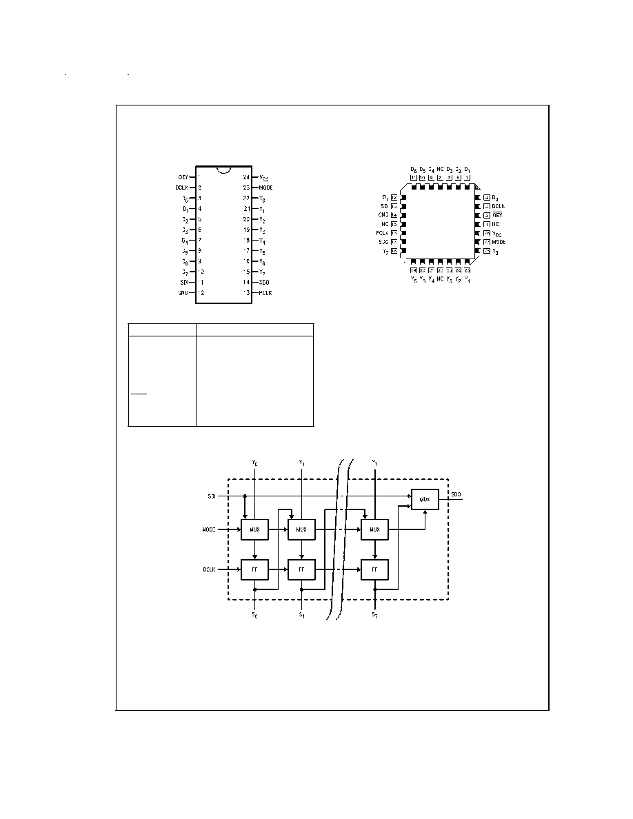
Connection Diagrams
Pin Names
Description
D
0
�D
7
Data Inputs
SDI
Serial Data Input
DCLK
Diagnostics Clock
MODE
Control Input
PCLK
Pipeline Register Clock
OEY
Output Enable Input
SDO
Serial Data Output
Y
0
�Y
7
Data Outputs
Diagnostic Register
Pin Assignment
for DIP and Flatpak
DS100251-1
Pin Assignment
for LCC
DS100251-2
DS100251-4
www.national.com
2

Block Diagram
Functional Description
Data transfers into the diagnostic register occur on the
LOW-to-HIGH transition of DCLK. Mode and SDI determine
what data source will be loaded. The pipeline register is
loaded on the LOW-to-HIGH transition of PCLK. Mode se-
lects whether the data source is the data input or the diag-
nostic register output. Because of the independence of the
clock inputs, data can be shifted in the diagnostic register via
DCLK and loaded into the pipeline register from the data in-
put via PCLK simultaneously, as long as no setup or hold
times are violated. This simultaneous operation is legal.
Function Table
Inputs
Outputs
Operation
SDI
MODE
DCLK
PCLK
SDO
Diagnostic Reg.
Pipeline Reg.
X
L
N
X
S7
SI
<
SI - 1,
NA
Serial Shift; D
7
�D
0
Disabled
SO
<
SD
I
X
L
X
N
S7
NA
PI
<
DI
Normal Load Pipeline Register
L
H
N
X
L
SI
<
YI
NA
Load Diagnostic Register from Y;
DI Disabled
X
H
X
N
SDI
NA
PI
<
SI
Load Pipeline Register from
Diagnostic Register
H
H
N
X
H
Hold
NA
Hold Diagnostic Register; DI
Enabled
H = HIGH Voltage Level
L = LOW Voltage Level
X = Immaterial
N = LOW-to-HIGH Clock Transition
DS100251-5
www.national.com
3

Absolute Maximum Ratings
(Note 1)
If Military/Aerospace specified devices are required,
please contact the National Semiconductor Sales Office/
Distributors for availability and specifications.
Supply Voltage (V
CC
)
-0.5V to +7.0V
DC Input Diode Current (I
IK
)
V
I
= -0.5V
-20 mA
V
I
= V
CC
+0.5V
+20 mA
DC Input Voltage (V
I
)
-0.5V to V
CC
+0.5V
DC Output Diode Current (I
OK
)
V
O
= -0.5V
-20 mA
V
O
= V
CC
+ 0.5V
+20 mA
DC Output Voltage (V
O
)
-0.5V to V
CC
+ 0.5V
DC Output Source
or Sink Current (I
O
)
�
50 mA
DC V
CC
or Ground Current
per Output Pin (I
CC
or I
GND
)
�
50 mA
Storage Temperature (T
STG
)
-65�C to +150�C
Junction Temperature (T
J
)
CDIP
175�C
Recommended Operating
Conditions
Supply Voltage (V
CC
)
'ACT
4.5V to 5.5V
Input Voltage (V
I
)
0V to V
CC
Output Voltage (V
O
)
0V to V
CC
Operating Temperature (T
A
)
54ACT
-55�C to +125�C
Minimum Input Edge Rate (
V/
t)
'ACT Devices
V
IN
from 0.8V to 2.0V
V
CC
@
4.5V, 5.5V
125 mV/ns
Note 1: Absolute maximum ratings are those values beyond which damage
to the device may occur. The databook specifications should be met, without
exception, to ensure that the system design is reliable over its power supply,
temperature, and output/input loading variables. National does not recom-
mend operation of FACT
TM
circuits outside databook specifications.
Note 2: All outputs loaded; thresholds on input associated with output under
test.
DC Characteristics for 'ACT Family Devices
54ACT
Symbol
Parameter
V
CC
T
A
=
Units
Conditions
(V)
-55�C to +125�C
Guaranteed Limits
V
IH
Minimum High Level
4.5
2.0
V
V
OUT
= 0.1V
Input Voltage
5.5
2.0
or V
CC
- 0.1V
V
IL
Maximum Low Level
4.5
0.8
V
OUT
= 0.1V
Input Voltage
5.5
0.8
or V
CC
- 0.1V
I
IN
Maximum Input
5.5
�
1.0
�A
V
IN
= V
CC
Leakage Current
I
OZ
Maximum TRI-STATE
5.5
�
1.0
�A
OE = V
IH
Leakage Current
V
OUT
= 0V, V
CC
I
CC
Maximum Quiescent
5.5
160
�A
V
IN
= V
CC
or GND
Supply Current
I
CCT
Maximum Additional
5.5
1.6
mA
V
IN
= V
CC
- 2.1V
I
CC
/Input
V
CC
= 5.5V
V
OH
Minimum HIGH
(Note 2)
V
IN
= V
IL
or V
IH
Level Output Voltage,
4.5
3.70
V
I
OH
= -24 mA
Y
0
�Y
7
Outputs
5.5
4.70
V
I
OH
=-24 mA
Minimum HIGH
Level Output Voltage,
4.5
3.70
V
I
OH
= -8 mA
D
0
�D
7
, SDO Outputs
5.5
4.70
V
I
OH
= -8 mA
V
OL
Maximum LOW
(Note 2)
V
IN
= V
IL
or V
IH
Level Output Voltage,
4.5
0.50
V
I
OL
= 24 mA
Y
0
�Y
7
Outputs
5.5
0.50
V
I
OL
= 24 mA
Maximum LOW
Level Output Voltage,
4.5
0.50
V
I
OL
= 8 mA
D
0
�D
7
, SDO Outputs
5.5
0.50
V
I
OL
= 8 mA
www.national.com
4

DC Characteristics for 'ACT Family Devices
(Continued)
54ACT
Symbol
Parameter
V
CC
T
A
=
Units
Conditions
(V)
-55�C to +125�C
Guaranteed Limits
I
OLD
Minimum Dynamic
V
OLD
= 1.65V Max
Output Current,
5.5
50
mA
Y
0
�Y
7
Outputs
I
OHD
Minimum Dynamic
V
OHD
= 3.85V Min
Output Current,
5.5
-50
mA
Y
0
�Y
7
Outputs
I
OLD
Minimum Dynamic
V
OLD
= 1.65V Max
Output Current,
5.5
32
mA
D
0
�D
7
, SDO Outputs
(Note 4)
I
OHD
Minimum Dynamic
V
OHD
= 3.85V Min
Output Current,
5.5
-32
mA
D
0
�D
7
, SDO Outputs
(Note 4)
Note 3: Maximum test duration 2.0 ms, one output loaded at a time.
Note 4: Test load 50 pF, 500
to ground.
Note 5: I
CC
for 54ACT
@
25�C is identical to 74ACT
@
25�C.
AC Electrical Characteristics
54ACT
V
CC
T
A
= -55�C
Fig.
Symbol
Parameter
(V)
to +125�C
Units
No.
(Note 6)
C
L
= 50 pF
Min
Max
t
PHL
Propagation Delay
5.0
2.5
10.0
ns
PCLK to Y
t
PLH
Propagation Delay
5.0
2.5
10.0
ns
PCLK to Y
t
PHL
Propagation Delay
5.0
3.5
12.0
ns
MODE to SDO
t
PLH
Propagation Delay
5.0
3.5
13.5
ns
MODE to SDO
t
PHL
Propagation Delay
5.0
3.0
11.5
ns
SDI to SDO
t
PLH
Propagation Delay
5.0
3.0
12.0
ns
SDI to SDO
t
PHL
Propagation Delay
5.0
3.5
14.0
ns
DCLK to SDO
t
PLH
Propagation Delay
5.0
3.5
15.5
ns
DCLK to SDO
t
PZL
Output Enable Time
5.0
2.5
12.0
ns
OEY to Y
n
t
PLZ
Output Disable Time
5.0
1.5
10.0
ns
OEY to Y
n
t
PZL
Output Enable Time
5.0
3.0
14.0
ns
DCLK to D
n
www.national.com
5