CLC532
High Speed 2:1 Analog Multiplexer
General Description
The CLC532 is a high speed 2:1 multiplexer with active input
and output stages. The CLC532 innovative design employs
a closed loop design which dramatically improves accuracy.
This monolithic device is constructed using an advanced
high performance bipolar process.
The CLC532 has been specifically designed to provide set-
tling times of 17ns to 0.01%. Fast settling time, coupled with
the adjustable bandwidth, and channel-to-channel isolation
is better than 80dB
@
10MHz. Low distortion (-80dBc) makes
the CLC532 an ideal choice for infrared and CCD imaging
systems and spurious signal levels make the CLC532 a very
suitable choice for both I/Q processors and receivers.
The
CLC532
is
offered
in
two
industrial
versions,
CLC532AJP\AJE, specified from -40∞C to +85∞C and pack-
aged in 14-pin plastic DIP14-pin and SOIC packages.
Enhanced Solutions (Military/Aerospace)
SMD Number: 5962-92035
*
Space level versions also available.
*
For more information, visit http://www.national.com/mil
Features
n
17ns 12-bit settling time to .01%
n
Low noise ≠ 32µVrms
n
High isolation ≠ 80dB
@
10MHz
n
Low distortion ≠ 80dBc
@
5MHz
n
Adjustable bandwidth≠190MHz(max)
Applications
n
Infrared system multiplexing
n
CCD sensor signals
n
Radar I/Q switching
n
High definition video HDTV
n
Test and calibration
Typical Application
Connection Diagram
Ordering Information
Package
Temperature Range
Industrial
Part Number
Package Marking
NSC Drawing
14-Pin Plastic DIP
-40∞C to +85∞C
CLC532AJP
CLC532AJP
N14E
14-Pin Plastic SOIC
-40∞C to +85∞C
CLC532AJE
CLC532AJE
M14A
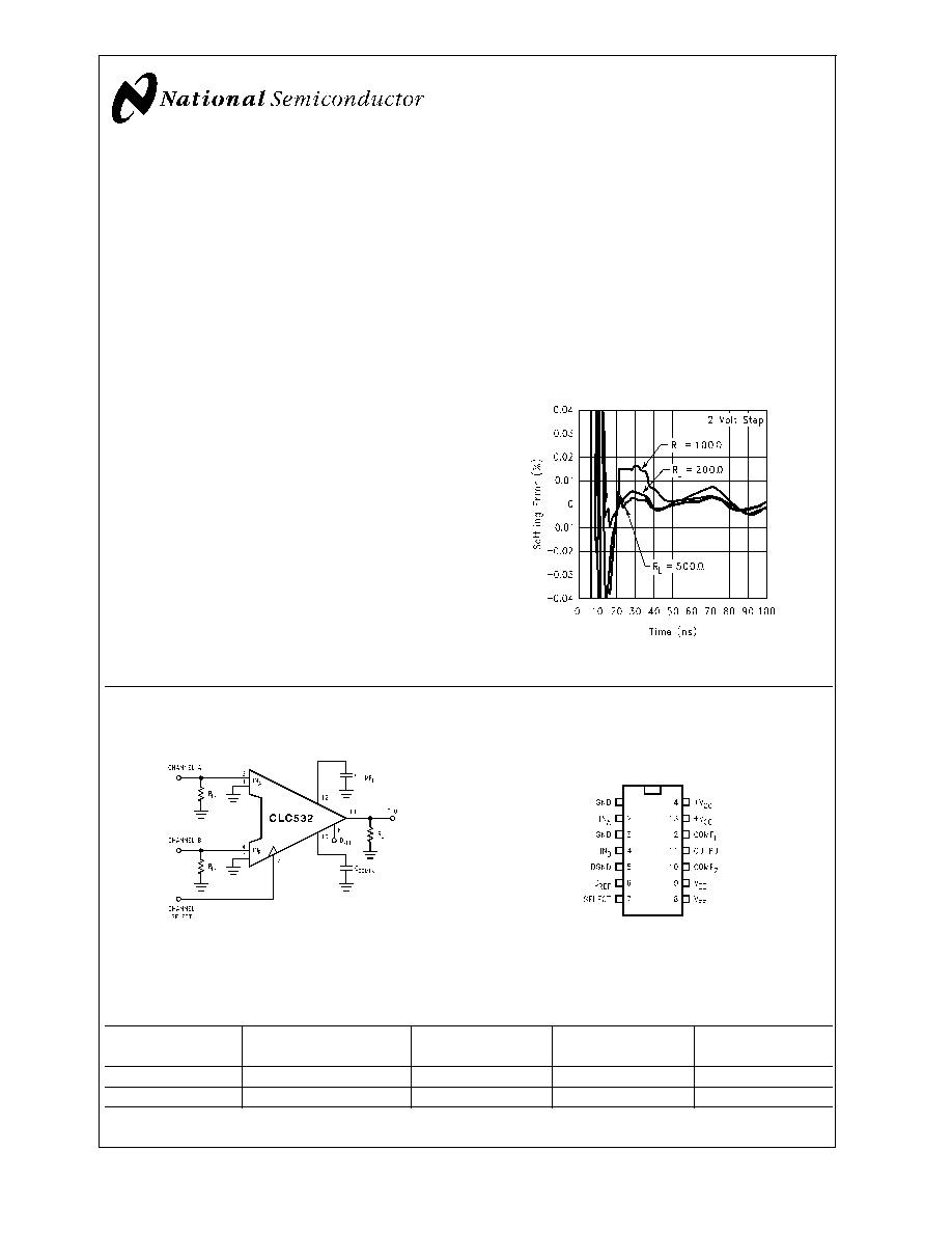
Settling Time vs. R
L
DS012716-24
DS012716-2
DS012716-4
Pinout
DIP & SOIC
December 2001
CLC532
High
Speed
2:1
Analog
Multiplexer
© 2001 National Semiconductor Corporation
DS012716
www.national.com

Absolute Maximum Ratings
(Note 1)
If Military/Aerospace specified devices are required,
please contact the National Semiconductor Sales Office/
Distributors for availability and specifications.
Positive Supply Voltage (+V
CC
)
-0.5V to +7.0V
Negative Supply Voltage (-V
EE
)
+0.5V to -7.0V
Differential Voltage between any two
GND's
200mV
Analog Input Voltage Range
-V
EE
to +V
CC
Digital Input Voltage Range
-V
EE
to +V
CC
Output Short Circuit Duration (Output
Shorted to GND)
Infinite
Operating Temperature Range
-40∞C to +85∞C
Storage Temperature Range
-65∞C to +150∞C
Lead Solder Duration (+300∞C)
10 sec
ESD Rating
<
500V
Operating Ratings
Positive Supply Voltage (+V
CC
)
+5v
Negative Supply Voltage (-V
EE
)
-5.2V or -5.0V
Differential Voltage between any two
GDN's
10mV
Analog Input Voltage Range
±
2V
SELECT Input Voltage Range (TTL
Mode)
0.0V to +3.0V
SELECT Input Voltage Range (ECL
Mode)
-2.0V to 0.0V
C
COMP
Range (Note 3)
5pF to 100pF
Thermal Resistance (
JC
)
MDIP
55∞C/W
SOIC
35∞C/W
Thermal Resistance (
JA
)
MDIP
100∞C/W
SOIC
105∞C/W
Electrical Characteristics
(+V
CC
= +5.0V; -V
EE
= -5.2V; R
IN
= 50
; R
L
= 500
; C
COMP
= 10pF; ECL Mode, pin 6 = NC)
Symbol
Parameter
Conditions
Typ
Max/Min Ratings
(Note 2)
Units
Case Temperature
CLC532AJP/AJE
+25∞C
-40∞C
+25∞C
+85∞C
Frequency Domain Response
SSBW
-3dB Bandwidth
V
OUT
<
0.1V
PP
190
140
140
110
MHz
LSBW
V
OUT
= 2V
PP
45
35
35
30
MHz
Gain Flatness
V
OUT
<
0.1V
PP
GFP
Peaking
0.1MHz to 200MHz
0.2
0.7
0.7
0.8
dB
GFR
Rolloff
0.1MHz to 100MHz
1.0
1.8
1.8
2.6
dB
LPD
Linear Phase Deviation
DC to 100MHz
2.0
deg
DG
Differential Gain
C
COMP
= 5pF; R
L
= 150
0.05
%
DP
Differential Phase
C
COMP
= 5pF; R
L
= 150
0.01
deg
CT10
Crosstalk Rejection
2V
PP
, 10MHz
80
75
75
74
dB
CT20
2V
PP
, 20MHz
74
69
69
68
dB
CT30
2V
PP
, 30MHz
68
63
63
62
dB
Time Domain Performance
TRS
Rise and Fall Time
0.5V Step
2.7
3.3
3.3
3.8
ns
TRL
2V Step
10
12.5
12.5
14.5
ns
TS14
Settling Time
2V Step; from 50% V
OUT
±
0.0025%
35
ns
TSP
±
0.01%
17
24
24
27
ns
TSS
±
0.1%
13
18
18
21
ns
OS
Overshoot
2.0V Step
2
5
5
6
%
SR
Slew Rate
160
130
130
110
V/µs
Switch Performance
SWT10
Channel to Channel Switching
Time (2V Step at Output)
50% SELECT to 10% V
OUT
5
7
7
8
ns
SWT90
50% SELECT to 90% V
OUT
15
20
20
23
ns
ST
Switching Transient
30
mV
Distortion And Noise Performance
HD2
2nd Harmonic Distortion
2V
PP
, 5MHz
80
67
67
67
dBc
HD3
3rd Harmonic Distortion
2V
PP
, 5MHz
86
68
68
68
dBc
Equivalent Input Noise
SNF
Spot Noise Voltage
>
1MHz
3.1
nV/
CLC532
www.national.com
2

Electrical Characteristics
(Continued)
(+V
CC
= +5.0V; -V
EE
= -5.2V; R
IN
= 50
; R
L
= 500
; C
COMP
= 10pF; ECL Mode, pin 6 = NC)
Symbol
Parameter
Conditions
Typ
Max/Min Ratings
(Note 2)
Units
Distortion And Noise Performance
INV
Integrated Noise
1MHz to 100MHz
32
42
42
46
µVrms
SNC
Spot Noise Current
3
pA/
Static And DC Performance
VOS
Analog Output Offset Voltage
(Note 5)
1
6.5
3.5
5.5
mV
DVIO
Temperature Coefficient
15
90
20
µV/∞C
VOSM
Analog Output Voltage Matching
TBD
mV
IBN
Analog Input Bias Current
50
250
120
120
µA
DIBN
Temperature Coefficient
0.3
2.0
0.8
µA/∞C
IBNM
Analog Input Bias Current
Matching (Note 5)
TBD
µA
RIN
Analog Input Resistance
200
90
120
120
k
CIN
Analog Input Capacitance
2
3.0
2.5
2.5
pF
GA
Gain Accuracy (Note 5)
±
2V
0.998
0.998
0.998
0.998
V/V
GAM
Gain Matching
±
2V
TBD
V/V
ILIN
Integral Endpoint Non-Linearity
±
1V (Full Scale)
0.02
0.05
0.03
0.03
%FS
VO
Output Voltage
No Load
±
3.4
2.4
2.8
2.8
V
IO
Output Current
45
20
30
30
mA
RO
Output Resistance
DC
1.5
4.0
2.5
2.5
Digital Input Performance
ECL Mode (Pin 6 Floating)
VIH1
Input Voltage Logic HIGH
-1.1
-1.1
-1.1
V
VIL1
Input Voltage Logic LOW
-1.5
-1.5
-1.5
V
IIH1
Input Current Logic HIGH
14
50
30
30
µA
IIL1
Input Current Logic LOW
50
270
110
110
µA
TTL Mode (pin 6 = +5V)
VIH2
Input Voltage Logic HIGH
2.0
2.0
2.0
V
VIL2
Input Voltage Logic LOW
0.8
0.8
0.8
V
IIH2
Input Current Logic HIGH
14
50
30
30
µA
IIL2
Input Current Logic LOW
50
270
110
110
µA
Power Requirements
ICC
Supply Current (+V
CC
= +5.0V)
(Note 5)
No Load
23
30
28
25
mA
IEE
Supply Current (-V
EE
= -5.2V)
(Note 5)
No Load
24
31
30
26
mA
PD
Nominal Power Dissipation
No Load
240
mW
PSRR
Power Supply Rejection Ratio
(Note 5)
73
60
64
64
dB
Note 1: "Absolute Maximum Ratings" are those values beyond which the safety of the device cannot be guaranteed. They are not meant to imply that the devices
should be operated at these limits. The table of "Electrical Characteristics" specifies conditions of device operation.
Note 2: Min/max ratings are based on product characterization and simulation. Individual parameters are tested as noted. Outgoing quality levels are determined
from tested parameters.
Note 3: The CLC532 does not require external C
COMP
capacitors for proper operation.
Note 4: Absolute maximum ratings are limiting values, to be applied individually, and beyond which the serviceability of the circuit maybe impaired. functional
operability under any of these conditions is not necessarily implied. Exposure to maximum ratings for extended periods may affect device reliability.
Note 5: AJ: 100% tested at +25∞C, sample tested at +85∞C
CLC532
www.national.com
3
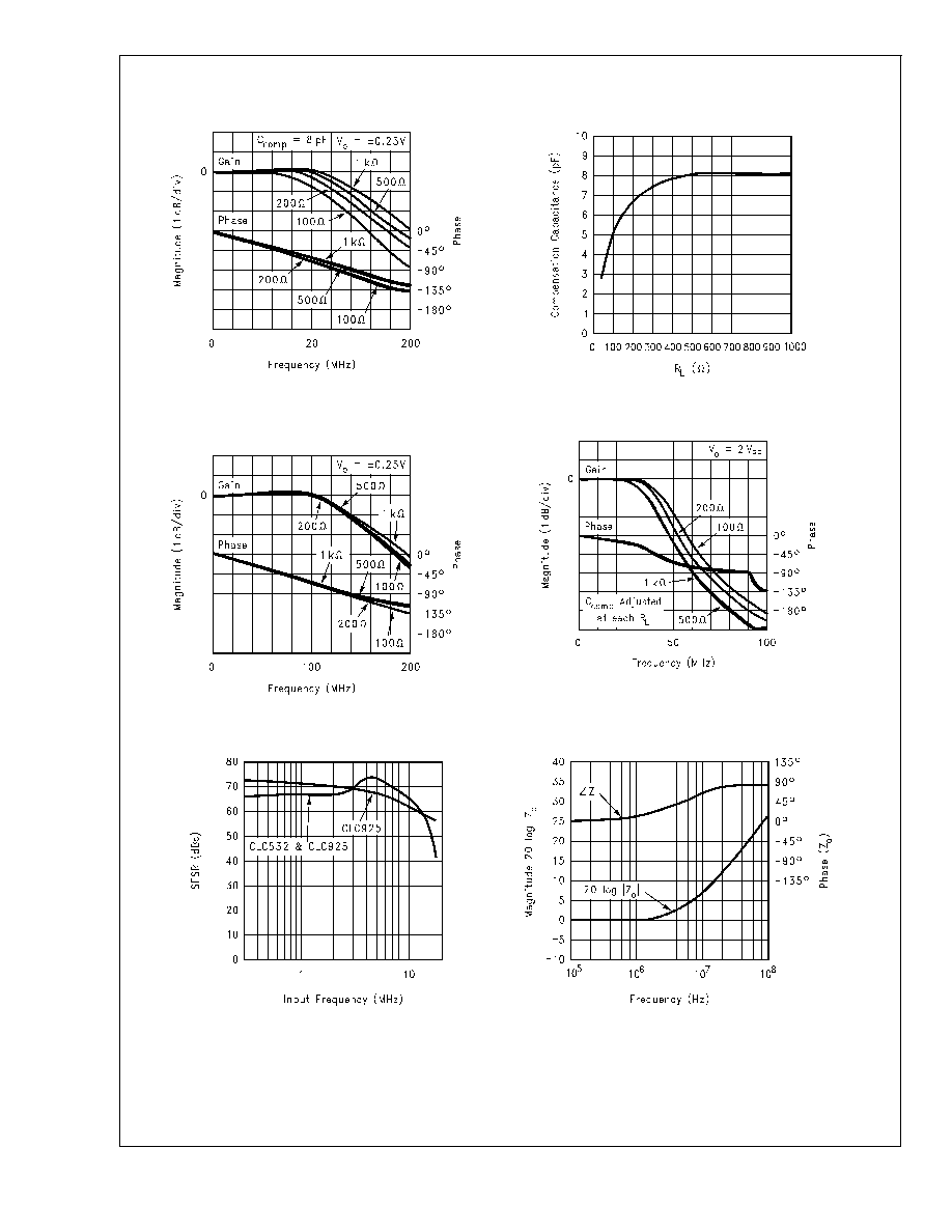
Typical Performance Characteristics
(+25∞C unless otherwise specified)
Small Signal/Phase vs. Load
DS012716-5
Recommended compensation Capacitance vs. Load
DS012716-6
Small Signal Gain/Phase vs. Load with Recommended
C
COMP
DS012716-7
Large Signal Frequency Response vs. Load
DS012716-8
SFRD vs. Input Frequency
DS012716-9
Output Impedance
DS012716-10
CLC532
www.national.com
4

Typical Performance Characteristics
(+25∞C unless otherwise specified) (Continued)
Channel to Channel Crosstalk
DS012716-11
Digitized Pulse Response
DS012716-12
Input Impedance
DS012716-13
Small Signal Pulse Response
DS012716-14
Large Signal Pulse Response vs. C
comp
DS012716-15
Large Signal Pulse Response vs. R
L
DS012716-16
CLC532
www.national.com
5