
54ACTQ646
Quiet Series Octal Transceiver/Register with 3-STATE
Outputs
General Description
The ACTQ646 consist of registered bus transceiver circuits,
with outputs, D-type flip-flops, and control circuitry providing
multiplexed transmission of data directly from the input bus
or from the internal storage registers. Data on the A or B bus
will be loaded into the respective registers on the
LOW-to-HIGH transition of the appropriate clock pin (CPAB
or CPBA). The four fundamental handling functions available
are illustrated in
Figures 1, 2, 3, 4.
The ACTQ utilizes FSC Quiet Series technology to guaran-
tee quiet output switching and improved dynamic threshold
performance. FACT Quiet Series
TM
features GTO
TM
output
control and undershoot corrector in addition to a split ground
bus for superior performance.
Features
n
Guaranteed simultaneous switching noise level and
dynamic threshold performance
n
Independent registers for A and B busses
n
Multiplexed real-time and stored data transfers
n
300 mil slim dual-in-line package
n
Outputs source/sink 24 mA
n
Faster prop delays than the standard AC/ACT646
n
4 kV minimum ESD immunity
n
Standard Microcircuit Drawing (SMD) 5962-9219601
Logic Symbols
Pin Descriptions
Pin Names
Description
A
0
≠A
7
Data Register A Inputs
Data Register A Outputs
B
0
≠B
7
Data Register B Inputs
Data Register B Outputs
CPAB,
CPBA
Clock Pulse Inputs
SAB, SBA
Transmit/Receive Inputs
GTO
TM
is a trademark of National Semiconductor Corporation
FACT
TM
and FACT Quiet Series
TM
are trademarks of Fairchild Semiconductor Corporation
DS100326-1
IEEE/IEC
DS100326-2
September 1998
54ACTQ646
Quiet
Series
Octal
T
ransceiver/Register
with
3-ST
A
T
E
Outputs
© 1998 National Semiconductor Corporation
DS100326
www.national.com

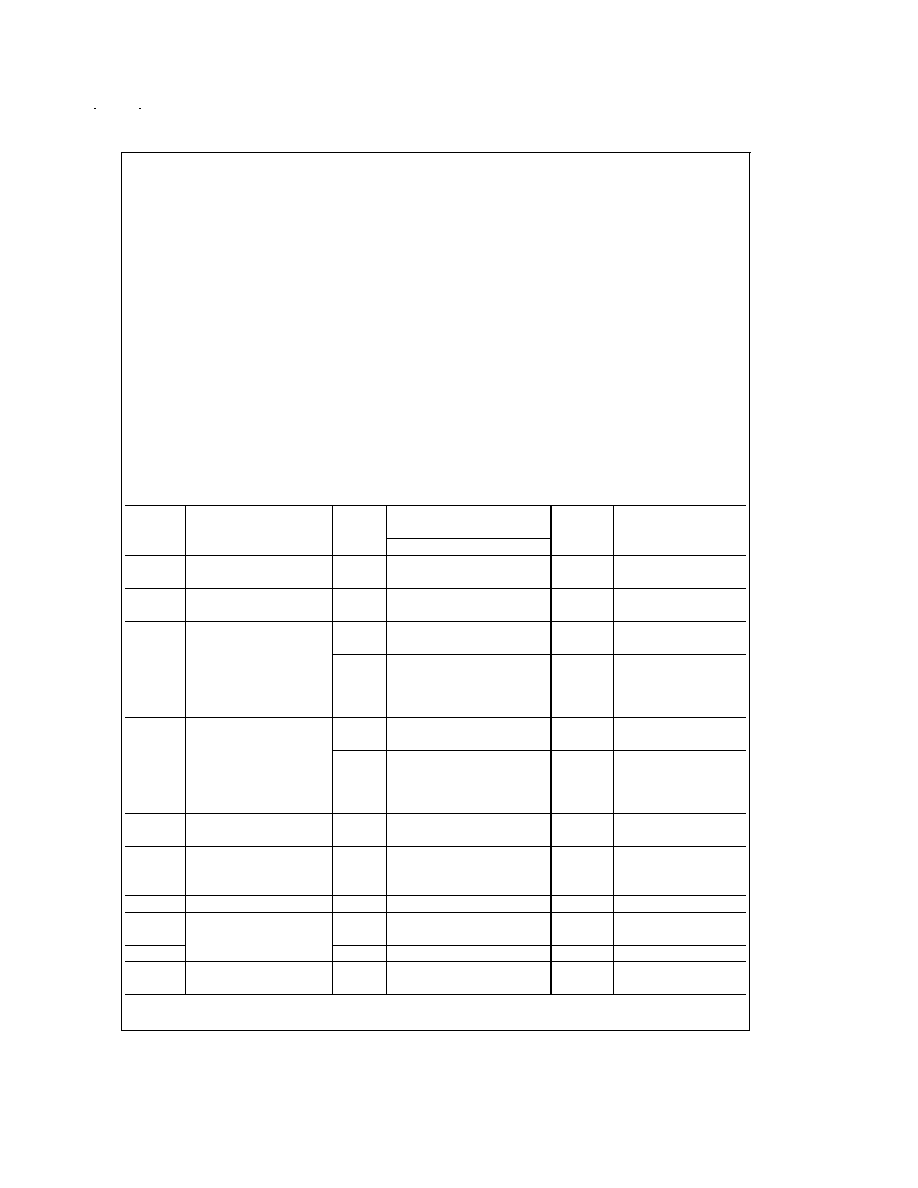
Function Table
Inputs
Data I/O (Note 1)
Function
G
DIR
CPAB
CPBA
SAB SBA
A
0
≠A
7
B
0
≠B
7
H
X
H or L
H or L
X
X
Isolation
H
X
N
X
X
X
Input
Input
Clock A
n
Data into A Register
H
X
X
N
X
X
Clock B
n
Data into B Register
L
H
X
X
L
X
A
n
to B
n
-- Real Time (Transparent Mode)
L
H
N
X
L
X
Input
Output
Clock A
n
Data into A Register
L
H
H or L
X
H
X
A Register to B
n
(Stored Mode)
L
H
N
X
H
X
Clock A
n
Data into A Register and Output to B
n
L
L
X
X
X
L
B
n
to A
n
-- Real Time (Transparent Mode)
L
L
X
N
X
L
Output
Input
Clock B
n
Data into B Register
L
L
X
H or L
X
H
B Register to A
n
(Stored Mode)
L
L
X
N
X
H
Clock B
n
Data into B Register and Output to A
n
H = HIGH Voltage Level
L = LOW Voltage Level
X = Immaterial
N = LOW-to-HIGH Transition
Note 1: The data output functions may be enabled or disabled by various signals at the G and DIR inputs. Data input functions are always enabled; i.e., data at the
bus pins will be stored on every LOW-to-HIGH transition of the appropriate clock inputs.
Real Time Transfer
A-Bus to B-Bus
DS100326-5
FIGURE 1.
Real Time Transfer
B-Bus to A-Bus
DS100326-6
FIGURE 2.
Storage from
Bus to Register
DS100326-7
FIGURE 3.
Transfer from
Register to Bus
DS100326-8
FIGURE 4.
www.national.com
3
Absolute Maximum Ratings
(Note 2)
If Military/Aerospace specified devices are required,
please contact the National Semiconductor Sales Office/
Distributors for availability and specifications.
Supply Voltage (V
CC
)
-0.5V to +7.0V
DC Input Diode Current (I
IK
)
V
I
= -0.5V
-20 mA
V
I
= V
CC
+ 0.5V
+20 mA
DC Input Voltage (V
I
)
-0.5V to V
CC
+ 0.5V
DC Output Diode Current (I
OK
)
V
O
= -0.5V
-20 mA
V
O
= V
CC
+ 0.5V
+20 mA
DC Output Voltage (V
O
)
-0.5V to V
CC
+ 0.5V
DC Output Source
or Sink Current (I
O
)
±
50 mA
DC V
CC
or Ground Current
per Output Pin (I
CC
or I
GND
)
±
50 mA
Storage Temperature (T
STG
)
-65∞C to +150∞C
DC Latch-Up Source
or Sink Current
±
300 mA
Junction Temperature (T
J
)
CDIP
175∞C
Recommended Operating
Conditions
Supply Voltage (V
CC
)
ACTQ
4.5V to 5.5V
Input Voltage (V
I
)
0V to V
CC
Output Voltage (V
O
)
0V to V
CC
Operating Temperature (T
A
)
54ACTQ
-55∞C to +125∞C
Minimum Input Edge Rate
V/
t
ACTQ Devices
V
IN
from 0.8V to 2.0V
V
CC
@
4.5V, 5.5V
125 mV/ns
Note 2: Absolute maximum ratings are those values beyond which damage
to the device may occur. The databook specifications should be met, without
exception, to ensure that the system design is reliable over its power supply,
temperature, and output/input loading variables. Fairchild does not recom-
mend operation of FACT
TM
circuits outside databook specifications.
DC Electrical Characteristics for ACTQ
Symbol
Parameter
V
CC
T
A
=
Units
Conditions
(V)
-55∞C to +125∞C
Guaranteed Limits
V
IH
Minimum High Level
4.5
2.0
V
V
OUT
= 0.1V
Input Voltage
5.5
2.0
or V
CC
- 0.1V
V
IL
Maximum Low Level
4.5
0.8
V
V
OUT
= 0.1V
Input Voltage
5.5
0.8
or V
CC
- 0.1V
V
OH
Minimum High Level
4.5
4.4
V
I
OUT
= -50 µA
Output Voltage
5.5
5.4
(Note 3)
V
IN
= V
IL
or V
IH
4.5
3.7
V
I
OH
= -24 mA
5.5
4.7
I
OH
= -24 mA
V
OL
Maximum Low Level
4.5
0.1
V
I
OUT
= 50 µA
Output Voltage
5.5
0.1
(Note 3)
V
IN
= V
IL
or V
IH
4.5
0.5
V
I
OL
= 24 mA
5.5
0.5
I
OL
= 24 mA
I
IN
Maximum Input
5.5
±
1.0
µA
V
I
= V
CC
, GND
Leakage Current
I
OZT
Maximum I/O
V
I
= V
IL
, V
IH
Leakage Current
5.5
±
10.0
µA
V
O
= V
CC
, GND
(A
n
, B
n
Inputs)
I
CCT
Maximum I
CC
/Input
5.5
1.6
mA
V
I
= V
CC
- 2.1V
(Note 4)
I
OLD
Minimum Dynamic
5.5
50
mA
V
OLD
= 1.65V Max
I
OHD
Output Current
5.5
-50
mA
V
OHD
= 3.85V Min
I
CC
Maximum Quiescent
5.5
160.0
µA
V
IN
= V
CC
Supply Current
or GND (Note 5)
www.national.com
5

