LP2952/LP2952A/LP2953/LP2953A
Adjustable Micropower Low-Dropout Voltage Regulators
General Description
The LP2952 and LP2953 are micropower voltage regulators
with very low quiescent current (130 µA typical at 1 mA load)
and very low dropout voltage (typ. 60 mV at light load and
470 mV at 250 mA load current). They are ideally suited for
battery-powered systems. Furthermore, the quiescent cur-
rent increases only slightly at dropout, which prolongs bat-
tery life.
The LP2952 and LP2953 retain all the desirable character-
istics of the LP2951, but offer increased output current,
additional features, and an improved shutdown function.
The internal crowbar pulls the output down quickly when the
shutdown is activated.
The error flag goes low if the output voltage drops out of
regulation.
Reverse battery protection is provided.
The internal voltage reference is made available for external
use, providing a low-T.C. reference with very good line and
load regulation.
The parts are available in DIP and surface mount packages.
Features
n
Output voltage adjusts from 1.23V to 29V
n
Guaranteed 250 mA output current
n
Extremely low quiescent current
n
Low dropout voltage
n
Extremely tight line and load regulation
n
Very low temperature coefficient
n
Current and thermal limiting
n
Reverse battery protection
n
50 mA (typical) output pulldown crowbar
n
5V and 3.3V versions available
LP2953 Versions Only
n
Auxiliary comparator included with CMOS/TTL
compatible output levels. Can be used for fault
detection, low input line detection, etc.
Applications
n
High-efficiency linear regulator
n
Regulator with under-voltage shutdown
n
Low dropout battery-powered regulator
n
Snap-ON/Snap-OFF regulator
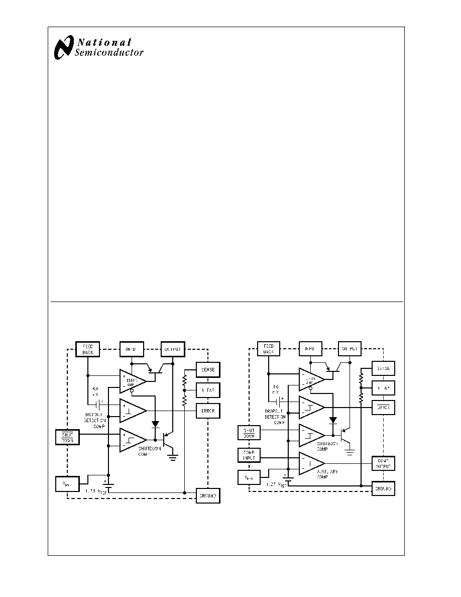
Block Diagrams
LP2952
01112701
LP2953
01112702
March 2005
LP2952/LP2952A/LP2953/LP2953A
Adjustable
Micropower
Low-Dropout
V
oltage
Regulators
© 2005 National Semiconductor Corporation
DS011127
www.national.com
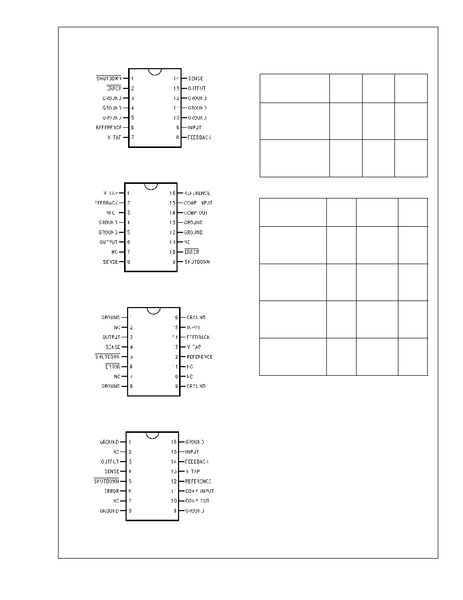
Pinout Drawings
LP2952
14-Pin DIP
01112711
LP2953
16-Pin DIP
01112713
LP2952
16-Pin SO
01112712
LP2953
16-Pin SO
01112714
Ordering Information
LP2952
Order
Number
Temp.
Range
(T
J
) ∞C
Package
NSC
Drawing
Number
LP2952IN,
LP2952AIN,
LP2952IN-3.3,
LP2952AIN-3.3
-40 to
+125
14-Pin
Molded
DIP
N14A
LP2952IM,
LP2952AIM,
LP2952IM-3.3,
LP2952AIM-3.3
-40 to
+125
16-Pin
Surface
Mount
M16A
LP2953
Order
Number
Temp.
Range
(T
J
) ∞C
Package
NSC
Drawing
Number
LP2953IN,
LP2953AIN,
LP2953IN-3.3,
LP2953AIN-3.3
-40 to
+125
16-Pin
Molded DIP
N16A
LP2953IM,
LP2953AIM,
LP2953IM-3.3,
LP2953AIM-3.3
-40 to
+125
16-Pin
Surface
Mount
M16A
LP2953AMJ/883
5962-9233601MEA
LP2953AMJ-QMLV
5962-9233601VEA
-55 to
+150
16-Pin
Ceramic DIP
J16A
LP2953AMWG/883
5962-9233601QXA
LP2953AMWG-QMLV
5962-9233601VXA
-55 to
+150
16-Pin
Ceramic
Surface
Mount
WG16A
LP2952/LP2952A/LP2953/LP2953A
www.national.com
2

Absolute Maximum Ratings
(Note 1)
If Military/Aerospace specified devices are required,
please contact the National Semiconductor Sales Office/
Distributors for availability and specifications.
Storage Temperature Range
-65∞C
T
A
+150∞C
Operating Temperature Range
LP2952I, LP2953I, LP2952AI,
LP2953AI, LP2952I-3.3,
LP2953I-3.3, LP2952AI-3.3,
LP2953AI-3.3
-40∞C
T
J
+125∞C
LP2953AM
-55∞C
T
A
+125∞C
Lead Temp. (Soldering, 5 seconds)
260∞C
Power Dissipation (Note 2)
Internally Limited
Maximum Junction Temperature
LP2952I, LP2953I, LP2952AI,
LP2953AI, LP2952I-3.3,
LP2953I-3.3, LP2952AI-3.3,
LP2953AI-3.3
+125∞C
LP2953AM
+150∞C
Input Supply Voltage
-20V to +30V
Feedback Input Voltage (Note 3)
-0.3V to +5V
Comparator Input Voltage (Note 4)
-0.3V to +30V
Shutdown Input Voltage (Note 4)
-0.3V to +30V
Comparator Output Voltage (Note
4)
-0.3V to +30V
ESD Rating (Note 15)
2 kV
Electrical Characteristics
Limits in standard typeface are for T
J
= 25∞C, bold typeface applies over the full
operating temperature range. Limits are guaranteed by production testing or correlation techniques using standard Statistical
Quality Control (SQC) methods. Unless otherwise specified: V
IN
= V
O
(NOM) + 1V, I
L
= 1 mA, C
L
= 2.2 µF for 5V parts and
4.7µF for 3.3V parts. Feedback pin is tied to V Tap pin, Output pin is tied to Output Sense pin.
3.3V Versions
Symbol
Parameter
Conditions
Typical
LP2952AI-3.3, LP2953AI-3.3
LP2952I-3.3, LP2953I-3.3
Units
Min
Max
Min
Max
V
O
Output Voltage
3.3
3.284
3.317
3.267
3.333
V
3.260
3.340
3.234
3.366
1 mA
I
L
250 mA
3.3
3.254
3.346
3.221
3.379
5V Versions
Symbol
Parameter
Conditions
Typical
LP2952AI, LP2953AI,
LP2952I, LP2953I
Units
LP2953AM (Note 17)
Min
Max
Min
Max
V
O
Output Voltage
5.0
4.975
5.025
4.950
5.050
V
4.940
5.060
4.900
5.100
1 mA
I
L
250 mA
5.0
4.930
5.070
4.880
5.120
All Voltage Options
Electrical Characteristics
Limits in standard typeface are for T
J
= 25∞C, bold typeface applies over the full operating temperature range. Limits are guar-
anteed by production testing or correlation techniques using standard Statistical Quality Control (SQC) methods. Unless other-
wise specified: V
IN
= V
O
(NOM) + 1V, I
L
= 1 mA, C
L
= 2.2 µF for 5V parts and 4.7µF for 3.3V parts. Feedback pin is tied to V
Tap pin, Output pin is tied to Output Sense pin.
Symbol
Parameter
Conditions
Typical LP2952AI, LP2953AI,
LP2952AI-3.3,
LP2953AI-3.3,
LP2953AM
(Notes 16, 17)
LP2952I, LP2953I,
LP2952I-3.3,
LP2953I-3.3
Units
Min
Max
Min
Max
REGULATOR
Output Voltage Temp.
Coefficient
(Note 5)
20
100
150
ppm/∞C
Output Voltage Line
Regulation
V
IN
= V
O
(NOM) + 1V to 30V
0.03
0.1
0.2
%
0.2
0.4
LP2952/LP2952A/LP2953/LP2953A
www.national.com
3

All Voltage Options
(Continued)
Electrical Characteristics
(Continued)
Limits in standard typeface are for T
J
= 25∞C, bold typeface applies over the full operating temperature range. Limits are guar-
anteed by production testing or correlation techniques using standard Statistical Quality Control (SQC) methods. Unless other-
wise specified: V
IN
= V
O
(NOM) + 1V, I
L
= 1 mA, C
L
= 2.2 µF for 5V parts and 4.7µF for 3.3V parts. Feedback pin is tied to V
Tap pin, Output pin is tied to Output Sense pin.
Symbol
Parameter
Conditions
Typical LP2952AI, LP2953AI,
LP2952AI-3.3,
LP2953AI-3.3,
LP2953AM
(Notes 16, 17)
LP2952I, LP2953I,
LP2952I-3.3,
LP2953I-3.3
Units
Min
Max
Min
Max
Output Voltage Load
Regulation (Note 6)
I
L
= 1 mA to 250 mA
0.04
0.16
0.20
%
I
L
= 0.1 mA to 1 mA
0.20
0.30
V
IN
≠V
O
Dropout Voltage
(Note 7)
I
L
= 1 mA
60
100
100
mV
150
150
I
L
= 50 mA
240
300
300
420
420
I
L
= 100 mA
310
400
400
520
520
I
L
= 250 mA
470
600
600
800
800
I
GND
Ground Pin Current
(Note 8)
I
L
= 1 mA
130
170
170
µA
200
200
I
L
= 50 mA
1.1
2
2
mA
2.5
2.5
I
L
= 100 mA
4.5
6
6
8
8
I
L
= 250 mA
21
28
28
33
33
I
GND
Ground Pin Current at
Dropout
V
IN
= V
O
(NOM) -0.5V
165
210
210
µA
I
L
= 100 µA
240
240
I
GND
Ground Pin Current at
Shutdown (Note 8)
V
SHUTDOWN
1.1V
105
140
140
µA
I
LIMIT
Current Limit
V
OUT
= 0
380
500
500
mA
530
530
Thermal Regulation
(Note 10)
0.05
0.2
0.2
%/W
e
n
Output Noise Voltage
(10 Hz to 100 kHz)
I
L
= 100 mA
C
L
= 4.7 µF
400
µV
RMS
C
L
= 33 µF
260
C
L
= 33 µF (Note 11)
80
V
REF
Reference Voltage
(Note 12)
1.230
1.215
1.245
1.205
1.255
V
1.205
1.255
1.190
1.270
Reference Voltage Line
Regulation
V
IN
= 2.5V to V
O
(NOM) + 1V
0.03
0.1
0.2
%
V
IN
= V
O
(NOM) + 1V to 30V
(Note 13)
0.2
0.4
Reference Voltage Load
Regulation
I
REF
= 0 to 200 µA
0.25
0.4
0.8
%
0.6
1.0
Reference Voltage
Temp. Coefficient
(Note 5)
20
ppm/∞C
LP2952/LP2952A/LP2953/LP2953A
www.national.com
4
All Voltage Options
(Continued)
Electrical Characteristics
(Continued)
Limits in standard typeface are for T
J
= 25∞C, bold typeface applies over the full operating temperature range. Limits are guar-
anteed by production testing or correlation techniques using standard Statistical Quality Control (SQC) methods. Unless other-
wise specified: V
IN
= V
O
(NOM) + 1V, I
L
= 1 mA, C
L
= 2.2 µF for 5V parts and 4.7µF for 3.3V parts. Feedback pin is tied to V
Tap pin, Output pin is tied to Output Sense pin.
Symbol
Parameter
Conditions
Typical LP2952AI, LP2953AI,
LP2952AI-3.3,
LP2953AI-3.3,
LP2953AM
(Notes 16, 17)
LP2952I, LP2953I,
LP2952I-3.3,
LP2953I-3.3
Units
Min
Max
Min
Max
I
B
(FB)
Feedback Pin Bias
Current
20
40
40
nA
60
60
I
O
(SINK) Output "OFF" Pulldown
Current
(Note 9)
30
30
mA
20
20
DROPOUT DETECTION COMPARATOR
I
OH
Output "HIGH" Leakage V
OH
= 30V
0.01
1
1
µA
2
2
V
OL
Output "LOW" Voltage
V
IN
= V
O
(NOM) - 0.5V
I
O
(COMP) = 400 µA
150
250
250
mV
400
400
V
THR
(MAX)
Upper Threshold
Voltage
(Note 14)
-60
-80
-35
-80
-35
mV
-95
-25
-95
-25
V
THR
(MIN)
Lower Threshold
Voltage
(Note 14)
-85
-110
-55
-110
-55
mV
-160
-40
-160
-40
HYST
Hysteresis
(Note 14)
15
mV
SHUTDOWN INPUT (Note 15)
V
OS
Input Offset
(Referred to V
REF
)
±
3
-7.5
7.5
-7.5
7.5
mV
Voltage
-10
10
-10
10
HYST
Hysteresis
6
mV
I
B
Input Bias
V
IN
(S/D) = 0V to 5V
10
-30
30
-30
-50
-30
50
nA
Current
-50
50
LP2953AM
10
-30
30
-75
75
AUXILIARY COMPARATOR (LP2953 Only)
V
OS
Input Offset Voltage
(Referred to V
REF
)
±
3
-7.5
7.5
-7.5
-10
7.5
10
mV
-10
10
LP2953AM
±
3
-7.5
7.5
-12
12
HYST
Hysteresis
6
mV
I
B
Input Bias Current
V
IN
(COMP) = 0V to 5V
10
-30
30
-30
-50
30
50
nA
-50
50
LP2953AM
10
-30
30
-75
75
I
OH
Output "HIGH" Leakage V
OH
= 30V
0.01
1
1
2
µA
V
IN
(COMP) = 1.3V
2
LP2953AM
0.01
1
2.2
V
OL
Output "LOW" Voltage
V
IN
(COMP) = 1.1V
150
250
250
400
mV
I
O
(COMP) = 400 µA
400
LP2953AM
150
250
420
LP2952/LP2952A/LP2953/LP2953A
www.national.com
5
All Voltage Options
(Continued)
Electrical Characteristics
(Continued)
Note 1: Absolute maximum ratings indicate limits beyond which damage to the component may occur. Electrical specifications do not apply when operating the
device outside of its rated operating conditions.
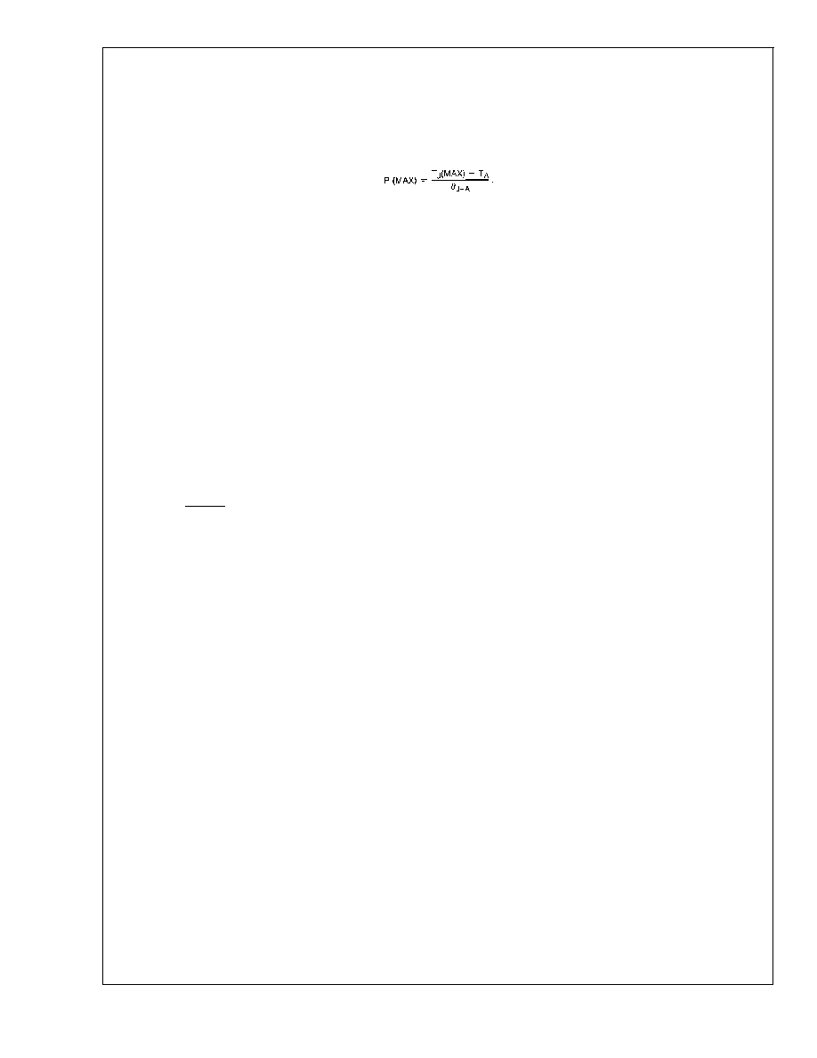
Note 2: The maximum allowable power dissipation is a function of the maximum junction temperature, T
J
(MAX), the junction-to-ambient thermal resistance,
J≠A
,
and the ambient temperature, T
A
. The maximum allowable power dissipation at any ambient temperature is calculated using the equation for P(MAX),
.
Exceeding the maximum allowable power dissipation will cause excessive die temperature, and the regulator will go into thermal shutdown. See APPLICATION
HINTS for additional information on heatsinking and thermal resistance.
Note 3: When used in dual-supply systems where the regulator load is returned to a negative supply, the output voltage must be diode-clamped to ground.
Note 4: May exceed the input supply voltage.
Note 5: Output or reference voltage temperature coefficient is defined as the worst case voltage change divided by the total temperature range.
Note 6: Load regulation is measured at constant junction temperature using low duty cycle pulse testing. Two separate tests are performed, one for the range of
100 µA to 1 mA and one for the 1 mA to 250 mA range. Changes in output voltage due to heating effects are covered by the thermal regulation specification.
Note 7: Dropout voltage is defined as the input to output differential at which the output voltage drops 100 mV below the value measured with a 1V differential. At
very low values of programmed output voltage, the input voltage minimum of 2V (2.3V over temperature) must be observed.
Note 8: Ground pin current is the regulator quiescent current. The total current drawn from the source is the sum of the ground pin current, output load current, and
current through the external resistive divider (if used).
Note 9: V
SHUTDOWN
1.1V, V
OUT
= V
O
(NOM).
Note 10: Thermal regulation is the change in output voltage at a time T after a change in power dissipation, excluding load or line regulation effects. Specifications
are for a 200 mA load pulse at V
IN
= V
O
(NOM)+15V (3W pulse) for T = 10 ms.
Note 11: Connect a 0.1 µF capacitor from the output to the feedback pin.
Note 12: V
REF
V
OUT
(V
IN
- 1V), 2.3V
V
IN
30V, 100 µA I
L
250 mA.
Note 13: Two separate tests are performed, one covering 2.5V
V
IN
V
O
(NOM)+1V and the other test for V
O
(NOM)+1V
V
IN
30V.
Note 14: Comparator thresholds are expressed in terms of a voltage differential at the Feedback terminal below the nominal reference voltage measured atV
IN
=
V
O
(NOM) + 1V. To express these thresholds in terms of output voltage change, multiply by the Error amplifier gain, which is V
OUT
/V
REF
= (R1 + R2)/R2(refer to
Figure 4).
Note 15: Human body model, 200 pF discharged through 1.5 k
.
Note 16: Drive Shutdown pin with TTL or CMOS-low level to shut regulator OFF, high level to turn regulator ON.
Note 17: A military RETS specification is available upon request. For more information on military products, please refer to the Mil-Aero web page at
http://www.national.com/appinfo/milaero/index.html.
LP2952/LP2952A/LP2953/LP2953A
www.national.com
6
Typical Performance Characteristics
Unless otherwise specified: V
IN
= 6V, I
L
= 1 mA, C
L
= 2.2
µF, V
SD
= 3V, T
A
= 25∞C, V
OUT
= 5V.
Quiescent Current
Quiescent Current
01112727
01112728
Ground Pin Current vs Load
Ground Pin Current
01112729
01112730
Ground Pin Current
Output Noise Voltage
01112731
01112732
LP2952/LP2952A/LP2953/LP2953A
www.national.com
7

Typical Performance Characteristics
Unless otherwise specified: V
IN
= 6V, I
L
= 1 mA, C
L
= 2.2 µF,
V
SD
= 3V, T
A
= 25∞C, V
OUT
= 5V. (Continued)
Ripple Rejection
Ripple Rejection
01112733
01112734
Ripple Rejection
Line Transient Response
01112735
01112736
Line Transient Response
Output Impedance
01112737
01112738
LP2952/LP2952A/LP2953/LP2953A
www.national.com
8

Typical Performance Characteristics
Unless otherwise specified: V
IN
= 6V, I
L
= 1 mA, C
L
= 2.2 µF,
V
SD
= 3V, T
A
= 25∞C, V
OUT
= 5V. (Continued)
Load Transient Response
Load Transient Response
01112739
01112740
Dropout Characteristics
Enable Transient
01112741
01112742
Enable Transient
Short-Circuit Output Current
and Maximum Output Current
01112743
01112744
LP2952/LP2952A/LP2953/LP2953A
www.national.com
9

Typical Performance Characteristics
Unless otherwise specified: V
IN
= 6V, I
L
= 1 mA, C
L
= 2.2 µF,
V
SD
= 3V, T
A
= 25∞C, V
OUT
= 5V. (Continued)
Feedback Bias Current
Feedback Pin Current
01112745
01112746
Error Output
Comparator Sink Current
01112747
01112748
Divider Resistance
Dropout Detection
Comparator Threshold
Voltages
01112749
01112750
LP2952/LP2952A/LP2953/LP2953A
www.national.com
10
Typical Performance Characteristics
Unless otherwise specified: V
IN
= 6V, I
L
= 1 mA, C
L
= 2.2 µF,
V
SD
= 3V, T
A
= 25∞C, V
OUT
= 5V. (Continued)
Thermal Regulation
Minimum Operating Voltage
01112751
01112752
Dropout Voltage
01112753
LP2952/LP2952A/LP2953/LP2953A
www.national.com
11
Schematic Diagram
01112706
Application Hints
HEATSINK REQUIREMENTS (Industrial Temperature
Range Devices)
The maximum allowable power dissipation for the LP2952/
LP2953 is limited by the maximum junction temperature
(+125∞C) and the external factors that determine how quickly
heat flows away from the part: the ambient temperature and
the junction-to-ambient thermal resistance for the specific
application.
The industrial temperature range (-40∞C
T
J
+125∞C)
parts are manufactured in plastic DIP and surface mount
packages which contain a copper lead frame that allows
heat to be effectively conducted away from the die, through
the ground pins of the IC, and into the copper of the PC
board. Details on heatsinking using PC board copper are
covered later.
To determine if a heatsink is required, the maximum power
dissipated by the regulator, P(max), must be calculated. It is
important to remember that if the regulator is powered from
a transformer connected to the AC line, the maximum
specified AC input voltage must be used (since this pro-
duces the maximum DC input voltage to the regulator).
Figure 1 shows the voltages and currents which are present
in the circuit. The formula for calculating the power dissi-
pated in the regulator is also shown in Figure 1:
LP2952/LP2952A/LP2953/LP2953A
www.national.com
12
Application Hints
(Continued)
The next parameter which must be calculated is the maxi-
mum allowable temperature rise, T
R
(max). This is calculated
by using the formula:
T
R
(max) = T
J
(max) - T
A
(max)
(J≠A)
= T
R
(max)/P(max)
where: T
J
(max)
is
the
maximum
allowable
junction
temperature
T
A
(max) is the maximum ambient temperature
Using the calculated values for T
R
(max) and P(max), the
required value for junction-to-ambient thermal resistance,
(J≠A)
, can now be found:
The heatsink is made using the PC board copper. The heat
is conducted from the die, through the lead frame (inside the
part), and out the pins which are soldered to the PC board.
The pins used for heat conduction are given in Table 1.
TABLE 1. Heat Conducting Pins
Part
Package
Pins
LP2952IN, LP2952AIN,
14-Pin DIP
3, 4, 5,
LP2952IN-3.3,
LP2952AIN-3.3
10, 11, 12
LP2953IN, LP2953AIN,
16-Pin DIP
4, 5, 12, 13
LP2953IN-3.3,
LP2953AIN-3.3
LP2952IM, LP2952AIM,
16-Pin Surface
Mount
1, 8, 9, 16
LP2952IM-3.3,
LP2952AIM-3.3,
LP2953IM, LP2953AIM,
LP2953IM-3.3,
LP2953AIM-3.3
Figure 2 shows copper patterns which may be used to
dissipate heat from the LP2952 and LP2953. Table 2 shows
some values of junction-to-ambient thermal resistance (
J≠A
)
for values of L and W for 1 oz. copper.
TABLE 2. Thermal Resistance for Various Copper
Heatsink Patterns
Package
L (in.)
H (in.)
J≠A
(∞C/W)
16-Pin DIP
1
0.5
70
2
1
60
3
1.5
58
4
0.19
66
6
0.19
66
14-Pin DIP
1
0.5
65
2
1
51
3
1.5
49
Surface Mount
1
0.5
83
2
1
70
3
1.5
67
6
0.19
69
4
0.19
71
2
0.19
73
HEATSINK REQUIREMENTS (Military Temperature
Range Devices)
The
maximum
allowable
power
dissipation
for
the
LP2953AMJ is limited by the maximum junction temperature
(+150∞C) and the two parameters that determine how quickly
heat flows away from the die: the ambient temperature and
the junction-to-ambient thermal resistance of the part.
01112707
FIGURE 1. P
TOTAL
= (V
IN
- V
OUT
) I
L
+ (V
IN
) I
G
Current/Voltage Diagram
01112708
* For best results, use L = 2H
** 14-Pin DIP is similar, refer to Table 1 for pins designated for
heatsinking.
FIGURE 2. Copper Heatsink Patterns
LP2952/LP2952A/LP2953/LP2953A
www.national.com
13
Application Hints
(Continued)
The military temperature range (-55∞C
T
J
+150∞C) parts
are manufactured in ceramic DIP packages which contain a
KOVAR lead frame (unlike the industrial parts, which have a
copper lead frame). The KOVAR material is necessary to
attain the hermetic seal required in military applications.
The KOVAR lead frame does not conduct heat as well as
copper, which means that the PC board copper can not be
used to significantly reduce the overall junction-to-ambient
thermal resistance in applications using the LP2953AMJ
part.
The power dissipation calculations for military applications
are done exactly the same as was detailed in the previous
section, with one important exception: the value for
(J≠A)
,
the junction-to-ambient thermal resistance, is fixed at
95∞C/W and can not be changed by adding copper foil
patterns to the PC board. This leads to an important fact:
The maximum allowable power dissipation in any application
using the LP2953AMJ is dependent only on the ambient
temperature:
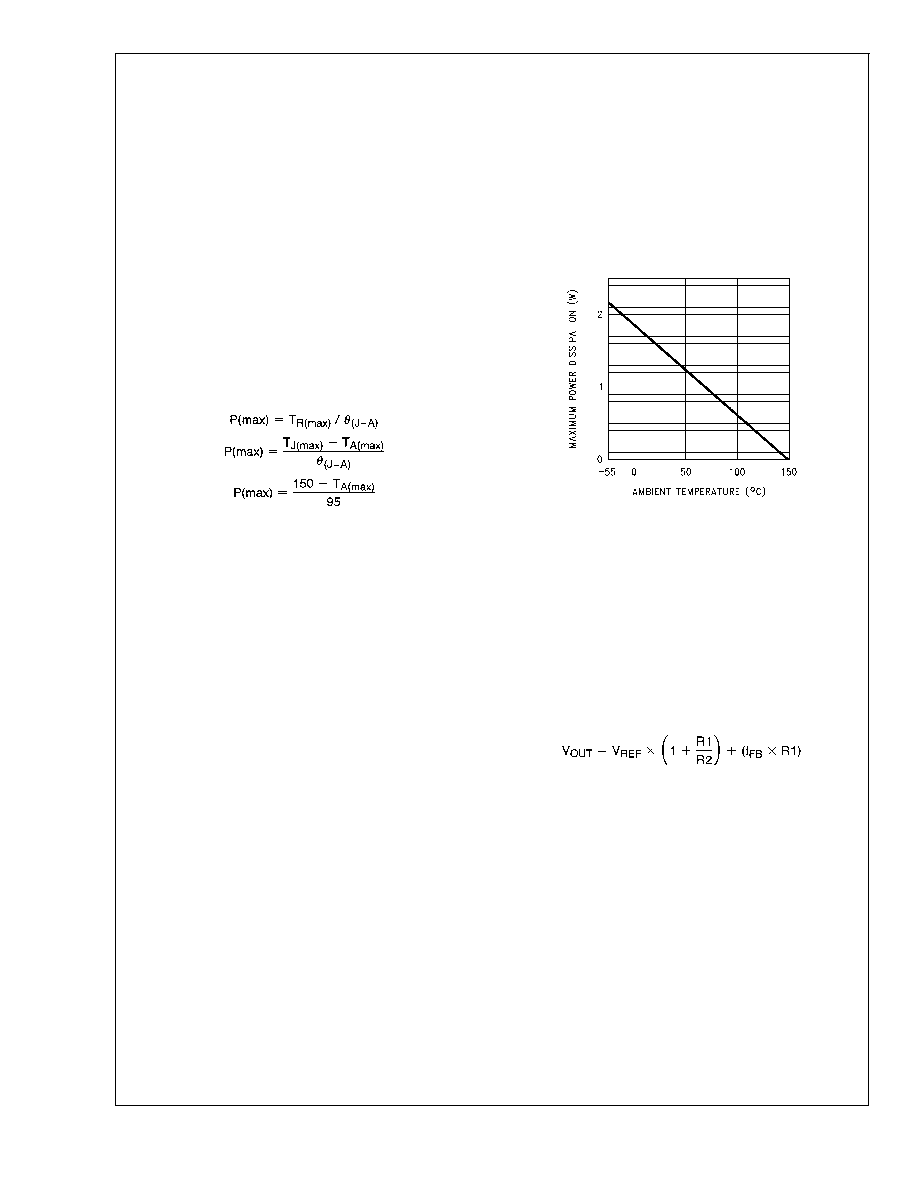
Figure 3 shows a graph of maximum allowable power dissi-
pation vs. ambient temperature for the LP2953AMJ, made
using the 95∞C/W value for
(J≠A)
and assuming a maximum
junction temperature of 150∞C (caution: the maximum ambi-
ent temperature which will be reached in a given application
must always be used to calculate maximum allowable power
dissipation).
EXTERNAL CAPACITORS
A 2.2 µF (or greater) capacitor is required between the
output pin and ground to assure stability when the output is
set to 5V. Without this capacitor, the part will oscillate. Most
type of tantalum or aluminum electrolytics will work here.
Film types will work, but are more expensive. Many alumi-
num electrolytics contain electrolytes which freeze at -30∞C,
which requires the use of solid tantalums below -25∞C. The
important parameters of the capacitor are an ESR of about
5
or less and a resonant frequency above 500 kHz (the
ESR may increase by a factor of 20 or 30 as the temperature
is reduced from 25∞C to -30∞C). The value of this capacitor
may be increased without limit.
At lower values of output current, less output capacitance is
required for stability. The capacitor can be reduced to
0.68 µF for currents below 10 mA or 0.22 µF for currents
below 1 mA.
Programming the output for voltages below 5V runs the error
amplifier at lower gains requiring more output capacitance
for stability. At 3.3V output, a minimum of 4.7 µF is required.
For the worst-case condition of 1.23V output and 250 mA of
load current, a 6.8 µF (or larger) capacitor should be used.
A 1 µF capacitor should be placed from the input pin to
ground if there is more than 10 inches of wire between the
input and the AC filter capacitor or if a battery input is used.
Stray capacitance to the Feedback terminal can cause insta-
bility. This problem is most likely to appear when using high
value external resistors to set the output voltage. Adding a
100 pF capacitor between the Output and Feedback pins
and increasing the output capacitance to 6.8 µF (or greater)
will cure the problem.
MINIMUM LOAD
When setting the output voltage using an external resistive
divider, a minimum current of 1 µA is recommended through
the resistors to provide a minimum load.
It should be noted that a minimum load current is specified in
several of the electrical characteristic test conditions, so this
value must be used to obtain correlation on these tested
limits.
PROGRAMMING THE OUTPUT VOLTAGE
The regulator may be pin-strapped for 5V operation using its
internal resistive divider by tying the Output and Sense pins
together and also tying the Feedback and 5V Tap pins
together.
Alternatively, it may be programmed for any voltage between
the 1.23V reference and the 30V maximum rating using an
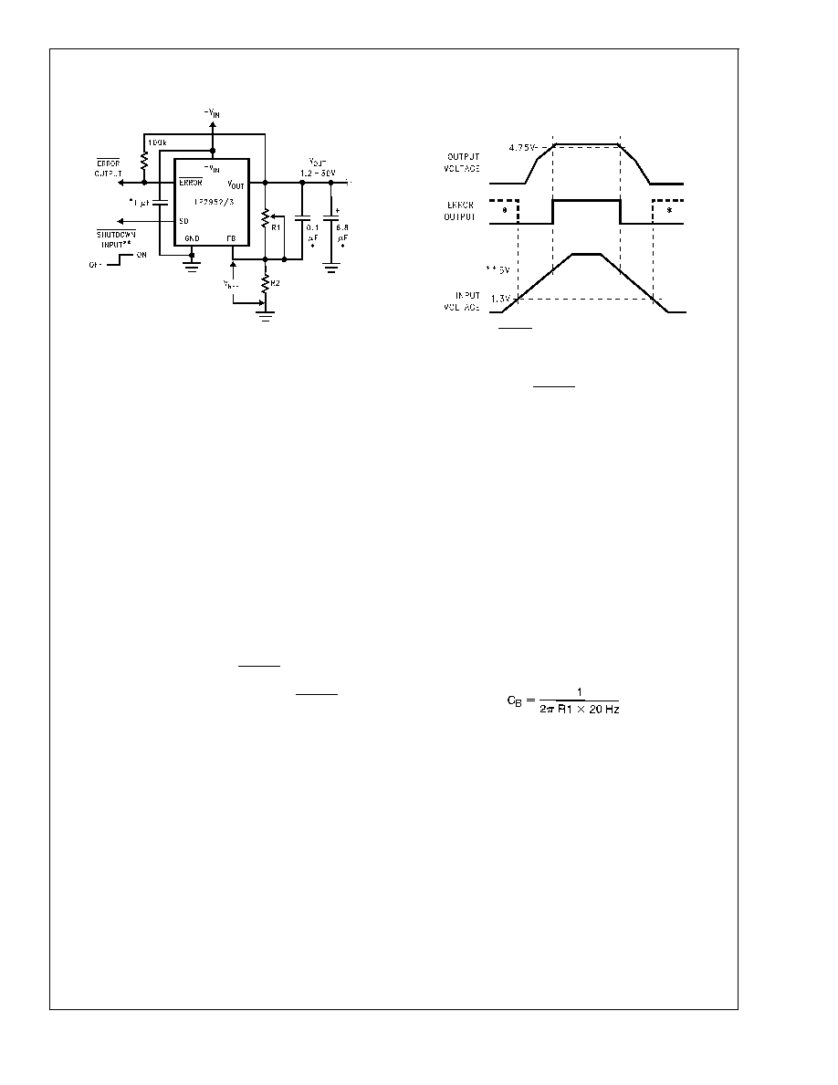
external pair of resistors (see Figure 4). The complete equa-
tion for the output voltage is:
where V
REF
is the 1.23V reference and I
FB
is the Feedback
pin bias current (-20 nA typical). The minimum recom-
mended load current of 1 µA sets an upper limit of 1.2 M
on
the value of R2 in cases where the regulator must work with
no load (see MINIMUM LOAD ). I
FB
will produce a typical 2%
error in V
OUT
which can be eliminated at room temperature
by trimming R1. For better accuracy, choosing R2 = 100 k
will reduce this error to 0.17% while increasing the resistor
program current to 12 µA. Since the typical quiescent current
is 120 µA, this added current is negligible.
01112726
FIGURE 3. Power Derating Curve for LP2953AMJ
LP2952/LP2952A/LP2953/LP2953A
www.national.com
14
Application Hints
(Continued)
DROPOUT VOLTAGE
The dropout voltage of the regulator is defined as the mini-
mum input-to-output voltage differential required for the out-
put voltage to stay within 100 mV of the output voltage
measured with a 1V differential. The dropout voltage is in-
dependent of the programmed output voltage.
DROPOUT DETECTION COMPARATOR
This comparator produces a logic "LOW" whenever the out-
put falls out of regulation by more than about 5%. This figure
results from the comparator's built-in offset of 60 mV divided
by the 1.23V reference (refer to block diagrams on page 1).
The 5% low trip level remains constant regardless of the
programmed output voltage. An out-of-regulation condition
can result from low input voltage, current limiting, or thermal
limiting.
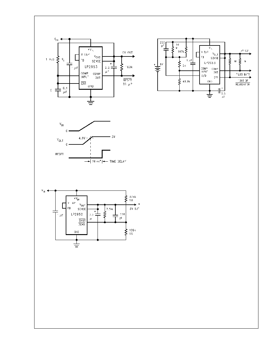
Figure 5 gives a timing diagram showing the relationship
between the output voltage, the ERROR output, and input
voltage as the input voltage is ramped up and down to a
regulator programmed for 5V output. The ERROR signal
becomes low at about 1.3V input. It goes high at about 5V
input, where the output equals 4.75V. Since the dropout
voltage is load dependent, the input voltage trip points will
vary with load current. The output voltage trip point does not
vary.
The comparator has an open-collector output which requires
an external pull-up resistor. This resistor may be connected
to the regulator output or some other supply voltage. Using
the regulator output prevents an invalid "HIGH" on the com-
parator output which occurs if it is pulled up to an external
voltage while the regulator input voltage is reduced below
1.3V. In selecting a value for the pull-up resistor, note that
while the output can sink 400 µA, this current adds to battery
drain. Suggested values range from 100 k
to 1 M. This
resistor is not required if the output is unused.
When V
IN
1.3V, the error flag pin becomes a high imped-
ance, allowing the error flag voltage to rise to its pull-up
voltage. Using V
OUT
as the pull-up voltage (rather than an
external 5V source) will keep the error flag voltage below
1.2V (typical) in this condition. The user may wish to divide
down the error flag voltage using equal-value resistors
(10 k
suggested) to ensure a low-level logic signal during
any fault condition, while still allowing a valid high logic level
during normal operation.
OUTPUT ISOLATION
The regulator output can be left connected to an active
voltage source (such as a battery) with the regulator input
power shut off, as long as the regulator ground pin is
connected to ground. If the ground pin is left floating,
damage to the regulator can occur if the output is pulled
up by an external voltage source.
REDUCING OUTPUT NOISE
In reference applications it may be advantageous to reduce
the AC noise present on the output. One method is to reduce
regulator bandwidth by increasing output capacitance. This
is relatively inefficient, since large increases in capacitance
are required to get significant improvement.
Noise can be reduced more effectively by a bypass capacitor
placed across R1 (refer to Figure 4). The formula for select-
ing the capacitor to be used is:
This gives a value of about 0.1 µF. When this is used, the
output capacitor must be 6.8 µF (or greater) to maintain
stability. The 0.1 µF capacitor reduces the high frequency
gain of the circuit to unity, lowering the output noise from 260
µV to 80 µV using a 10 Hz to 100 kHz bandwidth. Also, noise
is no longer proportional to the output voltage, so improve-
ments are more pronounced at high output voltages.
AUXILIARY COMPARATOR (LP2953 only)
The LP2953 contains an auxiliary comparator whose invert-
ing input is connected to the 1.23V reference. The auxiliary
comparator has an open-collector output whose electrical
characteristics are similar to the dropout detection compara-
tor. The non-inverting input and output are brought out for
external connections.
01112709
* See Application Hints
** Drive with TTL-low to shut down
FIGURE 4. Adjustable Regulator
01112710
* In shutdown mode, ERROR will go high if it has been pulled up to an
external supply. To avoid this invalid response, pull up to regulator output.
** Exact value depends on dropout voltage. (See Application Hints)
FIGURE 5. ERROR Output Timing
LP2952/LP2952A/LP2953/LP2953A
www.national.com
15
Application Hints
(Continued)
SHUTDOWN INPUT
A logic-level signal will shut off the regulator output when a
"LOW" (
<
1.2V) is applied to the Shutdown input.
To prevent possible mis-operation, the Shutdown input must
be actively terminated. If the input is driven from open-
collector logic, a pull-up resistor (20 k
to 100 k recom-
mended) should be connected from the Shutdown input to
the regulator input.
If the Shutdown input is driven from a source that actively
pulls high and low (like an op-amp), the pull-up resistor is not
required, but may be used.
If the shutdown function is not to be used, the cost of the
pull-up resistor can be saved by simply tying the Shutdown
input directly to the regulator input.
IMPORTANT: Since the Absolute Maximum Ratings state
that the Shutdown input can not go more than 0.3V below
ground, the reverse-battery protection feature which protects
the regulator input is sacrificed if the Shutdown input is tied
directly to the regulator input.
If reverse-battery protection is required in an application, the
pull-up resistor between the Shutdown input and the regula-
tor input must be used.
Typical Applications
Basic 5V Regulator
01112715
5V Current Limiter with Load Fault Indicator
01112716
* Output voltage equals +V
IN
minum dropout voltage, which varies with
output current. Current limits at a maximum of 380 mA (typical).
** Select R1 so that the comparator input voltage is 1.23V at the output
voltage which corresponds to the desired fault current value.
Low T.C. Current Sink
01112717
LP2952/LP2952A/LP2953/LP2953A
www.national.com
16
Typical Applications
(Continued)
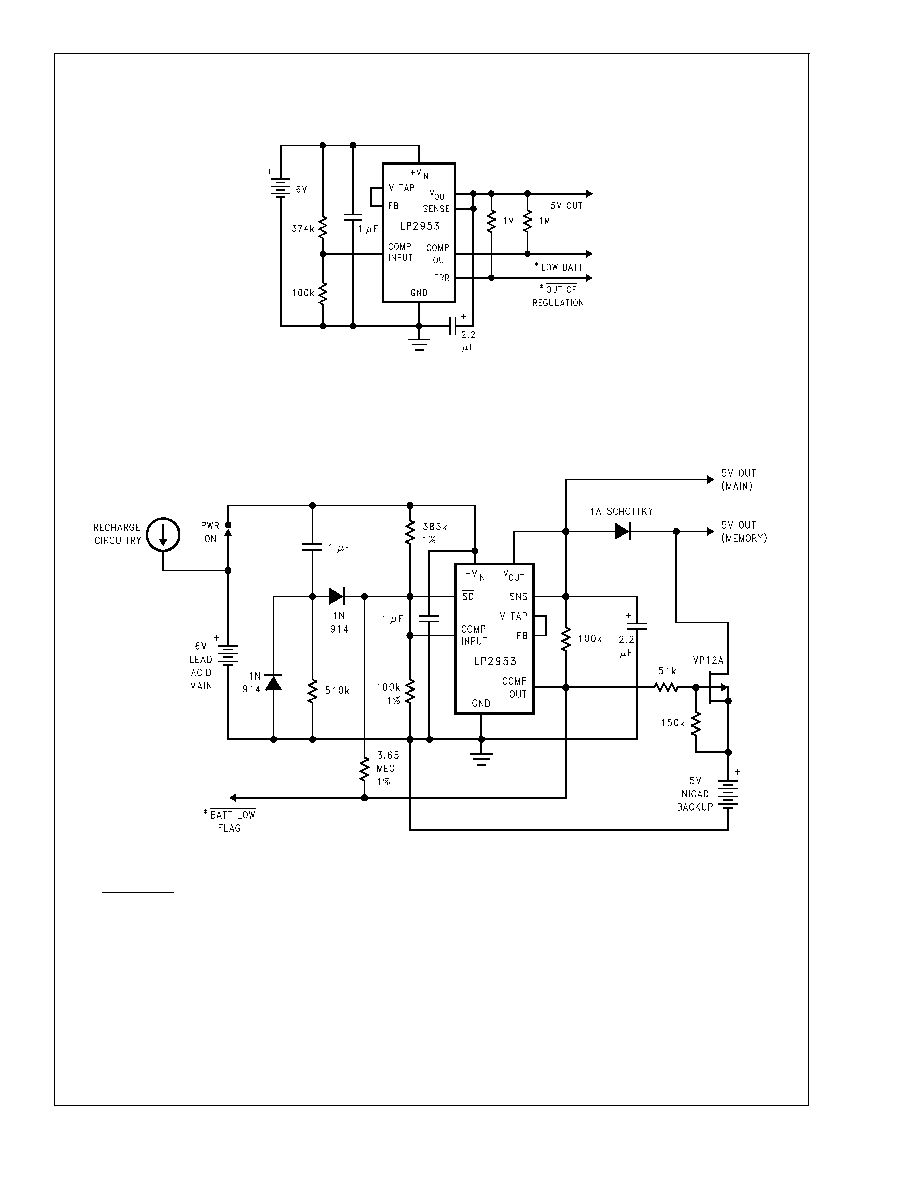
5V Regulator with Error Flags for
LOW BATTERY and OUT OF REGULATION
01112718
* Connect to Logic or µP control inputs.
LOW BATT flag warns the user that the battery has discharged down to about 5.8V, giving the user time to recharge the battery or power down some hardware
with high power requirements. The output is still in regulation at this time.
OUT OF REGULATION flag indicates when the battery is almost completely discharged, and can be used to initiate a power-down sequence.
5V Battery Powered Supply with Backup and Low Battery Flag
01112719
The circuit switches to the NI-CAD backup battery when the main battery voltage drops below about 5.6V, and returns to the main battery when its voltage is
recharged to about 6V.
The 5V MAIN output powers circuitry which requires no backup, and the 5V MEMORY output powers critical circuitry which can not be allowed to lose power.
* The BATTERY LOW flag goes low whenever the circuit switches to the NI-CAD backup battery.
LP2952/LP2952A/LP2953/LP2953A
www.national.com
17
Typical Applications
(Continued)
5V Regulator with Timed Power-On Reset
01112720
Timing Diagram for Timed Power-On Reset
01112721
* R
T
= 1 MEG, C
T
= 0.1 µF
5V Regulator with Snap-On/Snap-Off
Feature and Hysteresis
01112722
* Turns ON at V
IN
= 5.87V
Turns OFF at V
IN
= 5.64V
(for component values shown)
5V Regulator with Error Flags for
LOW BATTERY and OUT OF REGULATION
with SNAP-ON/SNAP-OFF Output
01112723
* Connect to Logic or µP control inputs.
OUTPUT has SNAP-ON/SNAP-OFF feature.
LOW BATT flag warns the user that the battery has discharged down to
about 5.8V, giving the user time to recharge the battery or shut down
hardware with high power requirements. The output is still in regulation at
this time.
OUT OF REGULATION flag goes low if the output goes below about 4.7V,
which could occur from a load fault.
OUTPUT has SNAP-ON/SNAP-OFF feature. Regulator snaps ON at about
5.7V input, and OFF at about 5.6V.
LP2952/LP2952A/LP2953/LP2953A
www.national.com
18

Typical Applications
(Continued)
5V Regulator with Timed Power-On Reset, Snap-On/Snap-Off Feature and Hysteresis
01112724
Timing Diagram
01112725
Td = (0.28) RC = 28 ms for components shown.
FIGURE 6.
LP2952/LP2952A/LP2953/LP2953A
www.national.com
19
Physical Dimensions
inches (millimeters)
unless otherwise noted
16-Pin Ceramic DIP
Order Number LP2953AMJ/883, 5962-9233601MEA, LP2953AMJ-QMLV, 5962-9233601VEA
NS Package Number J16A
16-Pin Surface Mount
Order Number LP2952IM, LP2952AIM, LP2952IM-3.3, LP2952AIM-3.3,
LP2953IM, LP2953AIM, LP2953IM-3.3 or LP2953AIM-3.3
NS Package Number M16A
LP2952/LP2952A/LP2953/LP2953A
www.national.com
20
Physical Dimensions
inches (millimeters) unless otherwise noted (Continued)
14-Pin Molded DIP
Order Number LP2952IN, LP2952AIN, LP2952IN-3.3 or LP2952AIN-3.3
NS Package Number N14A
16-Pin Molded DIP
Order Number LP2953IN, LP2953AIN, LP2953IN-3.3 or LP2953AIN-3.3
NS Package Number N16A
LP2952/LP2952A/LP2953/LP2953A
www.national.com
21
Physical Dimensions
inches (millimeters) unless otherwise noted (Continued)
16-Pin Ceramic Surface-Mount
Order Number LP2953AMWG/883, 5962-9233601QXA, LP2953AMWG-QMLV, 5962-9233601VXA
NS Package Number WG16A
National does not assume any responsibility for use of any circuitry described, no circuit patent licenses are implied and National reserves
the right at any time without notice to change said circuitry and specifications.
For the most current product information visit us at www.national.com.
LIFE SUPPORT POLICY
NATIONAL'S PRODUCTS ARE NOT AUTHORIZED FOR USE AS CRITICAL COMPONENTS IN LIFE SUPPORT DEVICES OR SYSTEMS
WITHOUT THE EXPRESS WRITTEN APPROVAL OF THE PRESIDENT AND GENERAL COUNSEL OF NATIONAL SEMICONDUCTOR
CORPORATION. As used herein:
1. Life support devices or systems are devices or systems
which, (a) are intended for surgical implant into the body, or
(b) support or sustain life, and whose failure to perform when
properly used in accordance with instructions for use
provided in the labeling, can be reasonably expected to result
in a significant injury to the user.
2. A critical component is any component of a life support
device or system whose failure to perform can be reasonably
expected to cause the failure of the life support device or
system, or to affect its safety or effectiveness.
BANNED SUBSTANCE COMPLIANCE
National Semiconductor manufactures products and uses packing materials that meet the provisions of the Customer Products
Stewardship Specification (CSP-9-111C2) and the Banned Substances and Materials of Interest Specification (CSP-9-111S2) and contain
no ``Banned Substances'' as defined in CSP-9-111S2.
National Semiconductor
Americas Customer
Support Center
Email: new.feedback@nsc.com
Tel: 1-800-272-9959
National Semiconductor
Europe Customer Support Center
Fax: +49 (0) 180-530 85 86
Email: europe.support@nsc.com
Deutsch Tel: +49 (0) 69 9508 6208
English
Tel: +44 (0) 870 24 0 2171
FranÁais Tel: +33 (0) 1 41 91 8790
National Semiconductor
Asia Pacific Customer
Support Center
Email: ap.support@nsc.com
National Semiconductor
Japan Customer Support Center
Fax: 81-3-5639-7507
Email: jpn.feedback@nsc.com
Tel: 81-3-5639-7560
www.national.com
LP2952/LP2952A/LP2953/LP2953A
Adjustable
Micropower
Low-Dropout
V
oltage
Regulators