DS26LS31C/DS26LS31M
Quad High Speed Differential Line Driver
General Description
The DS26LS31 is a quad differential line driver designed for
digital
data
transmission
over
balanced
lines.
The
DS26LS31 meets all the requirements of EIA Standard
RS-422 and Federal Standard 1020. It is designed to provide
unipolar differential drive to twisted-pair or parallel-wire
transmission lines.
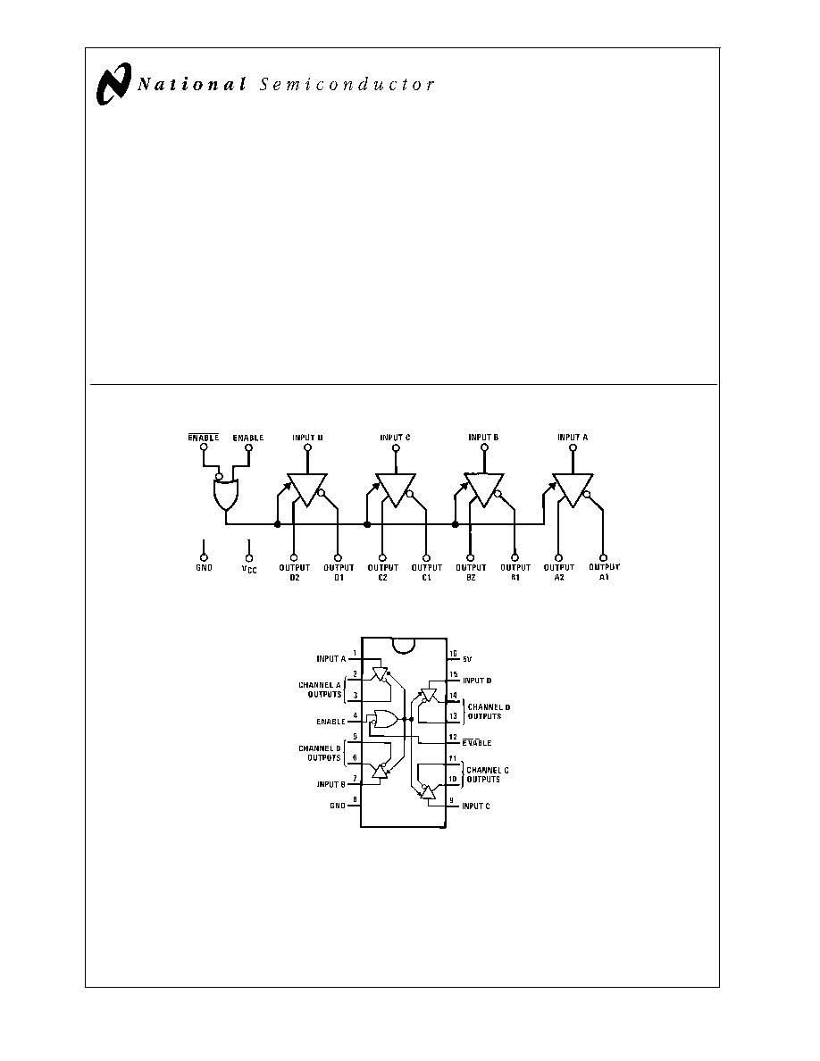
The circuit provides an enable and disable function common
to all four drivers. The DS26LS31 features TRI-STATE
Æ
out-
puts and logically ANDed complementary outputs. The in-
puts are all LS compatible and are all one unit load.
Features
n
Output skew -- 2.0 ns typical
n
Input to output delay -- 10 ns typical
n
Operation from single 5V supply
n
Outputs won't load line when V
CC
= 0V
n
Four line drivers in one package for maximum package
density
n
Output short-circuit protection
n
Complementary outputs
n
Meets the requirements of EIA Standard RS-422
n
Pin compatible with AM26LS31
n
Available in military and commercial temperature range
Logic and Connection Diagrams
TRI-STATE
Æ
is a registered trademark of National Semiconductor Corporation.
DS005778-1
Dual-In-Line Package
DS005778-2
Top View
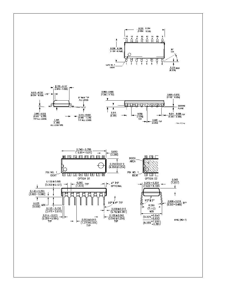
Order Number DS26LS31CM, or DS26LS31CN
See NS Package M16A or N16E
For Complete Military Product Specifications,
refer to the appropriate SMD or MDS.
Order Number DS26LS31MJ/883, DS26LS31ME/883 or DS26LS31MW/883
See NS Package E20A, J16A or W16A
June 1998
DS26LS31C/DS26LS31M
Quad
High
Speed
Differential
Line
Driver
© 2000 National Semiconductor Corporation
DS005778
www.national.com

Absolute Maximum Ratings
(Note 2)
If Military/Aerospace specified devices are required,
please contact the National Semiconductor Sales Office/
Distributors for availability and specifications.
Supply Voltage
7V
Input Voltage
7V
Output Voltage
5.5V
Output Voltage (Power OFF)
-0.25 to 6V
Maximum Power Dissipation (Note 1) at 25∞C
Cavity Package
1509 mW
Molded DIP Package
1476 mW
SO Package
1051 mW
Operating Conditions
Min
Max
Units
Supply Voltage, V
CC
DS26LS31M
4.5
5.5
V
DS26LS31
4.75
5.25
V
Temperature, T
A
DS26LS31M
-55
+125
∞C
DS26LS31
0
+70
∞C
Note 1: Derate cavity package 10.1 mW/∞C above 25∞C; derate molded DIP
package 11.9 mW/∞C above 25∞C; derate SO package 8.41 mW/∞C above
25∞C.
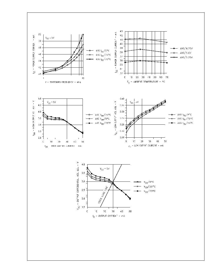
Electrical Characteristics
(Notes 3, 4, 5)
Symbol
Parameter
Conditions
Min
Typ
Max
Units
V
OH
Output High Voltage
I
OH
= -20 mA
2.5
V
V
OL
Output Low Voltage
I
OL
= 20 mA
0.5
V
V
IH
Input High Voltage
2.0
V
V
IL
Input Low Voltage
0.8
V
I
IL
Input Low Current
V
IN
= 0.4V
-40
-200
µA
I
IH
Input High Current
V
IN
= 2.7V
20
µA
I
I
Input Reverse Current
V
IN
= 7V
0.1
mA
I
O
TRI-STATE Output Current
V
O
= 2.5V
20
µA
V
O
= 0.5V
-20
µA
V
CL
Input Clamp Voltage
I
IN
= -18 mA
-1.5
V
I
SC
Output Short-Circuit Current
-30
-150
mA
I
CC
Power Supply Current
All Outputs Disabled
35
60
mA
or Active
Switching Characteristics
V
CC
= 5V, T
A
= 25∞C
Symbol
Parameter
Conditions
Min
Typ
Max
Units
t
PLH
Input to Output
C
L
= 30 pF
10
15
ns
t
PHL
Input to Output
C
L
= 30 pF
10
15
ns
Skew
Output to Output
C
L
= 30 pF
2.0
6.0
ns
t
LZ
Enable to Output
C
L
= 10 pF, S2 Open
15
35
ns
t
HZ
Enable to Output
C
L
= 10 pF, S1 Open
15
25
ns
t
ZL
Enable to Output
C
L
= 30 pF, S2 Open
20
30
ns
t
ZH
Enable to Output
C
L
= 30 pF, S1 Open
20
30
ns
Note 2: "Absolute Maximum Ratings" are those values beyond which the safety of the device cannot be guaranteed. They are not meant to imply that the devices
should be operated at these limits. The tables of "Electrical Characteristics" provide conditions for actual device operation.
Note 3: Unless otherwise specified min/max limits apply across the -55∞C to +125∞C temperature range for the DS726LS31M and across the 0∞C to +70∞C range
for the DS26LS31. All typicals are given for V
CC
= 5V and T
A
= 25∞C.
Note 4: All currents into device pins are positive; all currents out of device pins are negative. All voltages are referenced to ground unless otherwise specified.
Note 5: Only one output at a time should be shorted.
DS26LS31C/DS26LS31M
www.national.com
2
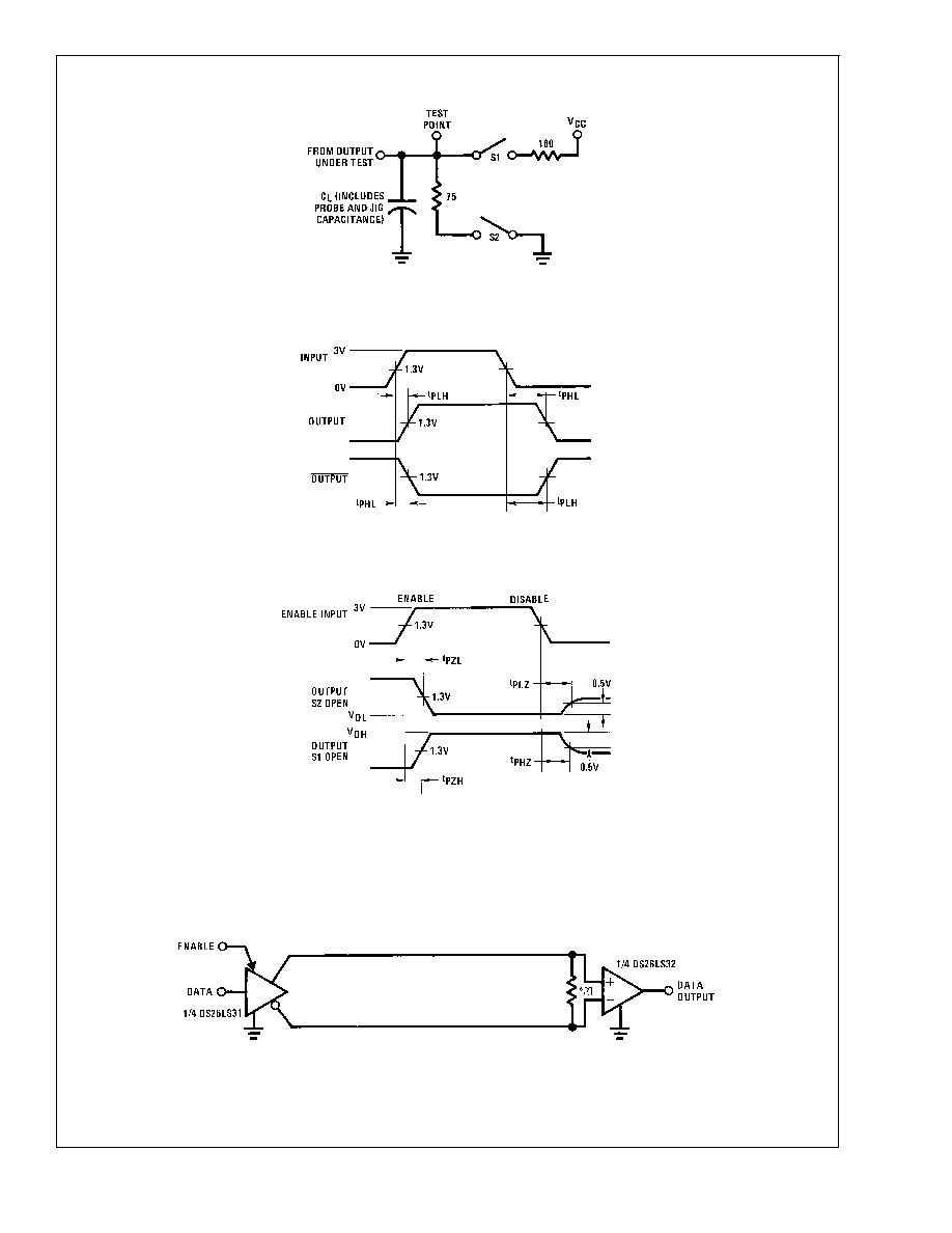
AC Test Circuit and Switching Time Waveforms
Typical Applications
DS005778-3
S1 and S2 of load circuit are closed except where shown.
FIGURE 1. AC Test Circuit
DS005778-4
f = 1 MHz, t
r
15 ns, t
f
6 ns
FIGURE 2. Propagation Delays
DS005778-5
f = 1 MHz, t
r
15 ns, t
f
6 ns
FIGURE 3. Enable and Disable Times
Two-Wire Balanced System, RS-422
DS005778-6
Note 6: R
T
is optional although highly recommended to reduce reflection.
DS26LS31C/DS26LS31M
www.national.com
3