
54AC520
∑
54ACT520
8-Bit Identity Comparator
General Description
The 'AC/'ACT520 are expandable 8-bit comparators. They
compare two words of up to eight bits each and provide a
LOW output when the two words match bit for bit. The
expansion input I
A = B
also serves as an active LOW enable
input.
Features
n
Compares two 8-bit words in 6.5 ns typ
n
Expandable to any word length
n
20-pin package
n
Outputs source/sink 24 mA
n
'ACT520 has TTL-compatible inputs
n
Standard Microcircuit Drawing (SMD)
54AC520: 5962-90916
54ACT520: 5962-89793
Logic Symbols
Pin Names
Description
A
0
≠A
7
Word A Inputs
B
0
≠B
7
Word B Inputs
T
A = B
Expansion or Enable Input
O
A = B
Identity Output
FACT
TM
is a trademark of Fairchild Semiconductor Corporation.
DS100234-1
IEEE/IEC
DS100234-4
September 1998
54AC520
∑
54ACT520
8-Bit
Identity
Comparator
© 2001 National Semiconductor Corporation
DS100234
www.national.com

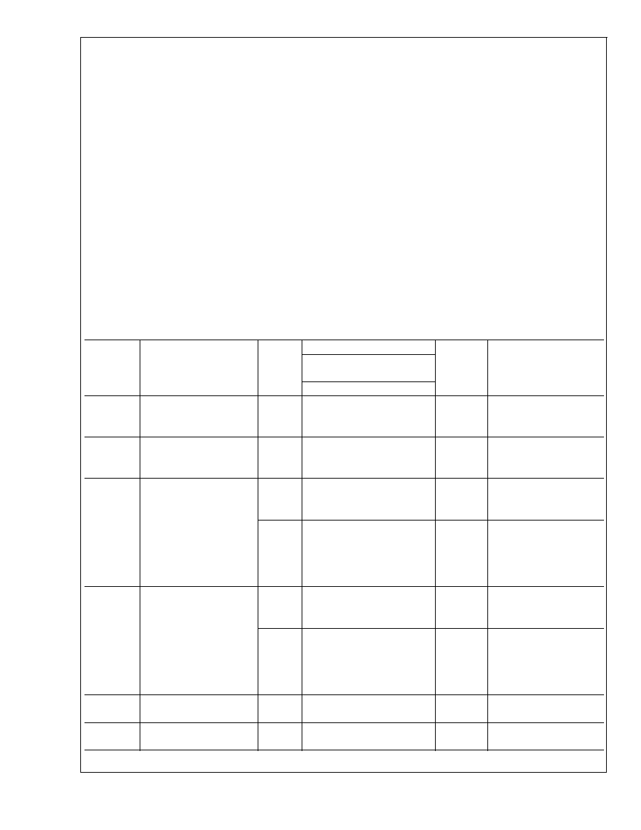
Connection Diagrams
Inputs
Outputs
I
A = B
A, B
O
A = B
L
A = B
*
L
L
A
B
H
H
A = B
*
H
H
A
B
H
H = HIGH Voltage Level
L = LOW Voltage Level
*
A
0
= B
0
, A
1
= B
1
, A
2
= B
2
, etc.
Pin Assignment
for DIP and Flatpak
DS100234-2
Pin Assignment
for LCC
DS100234-3
54AC520
∑
54ACT520
www.national.com
2
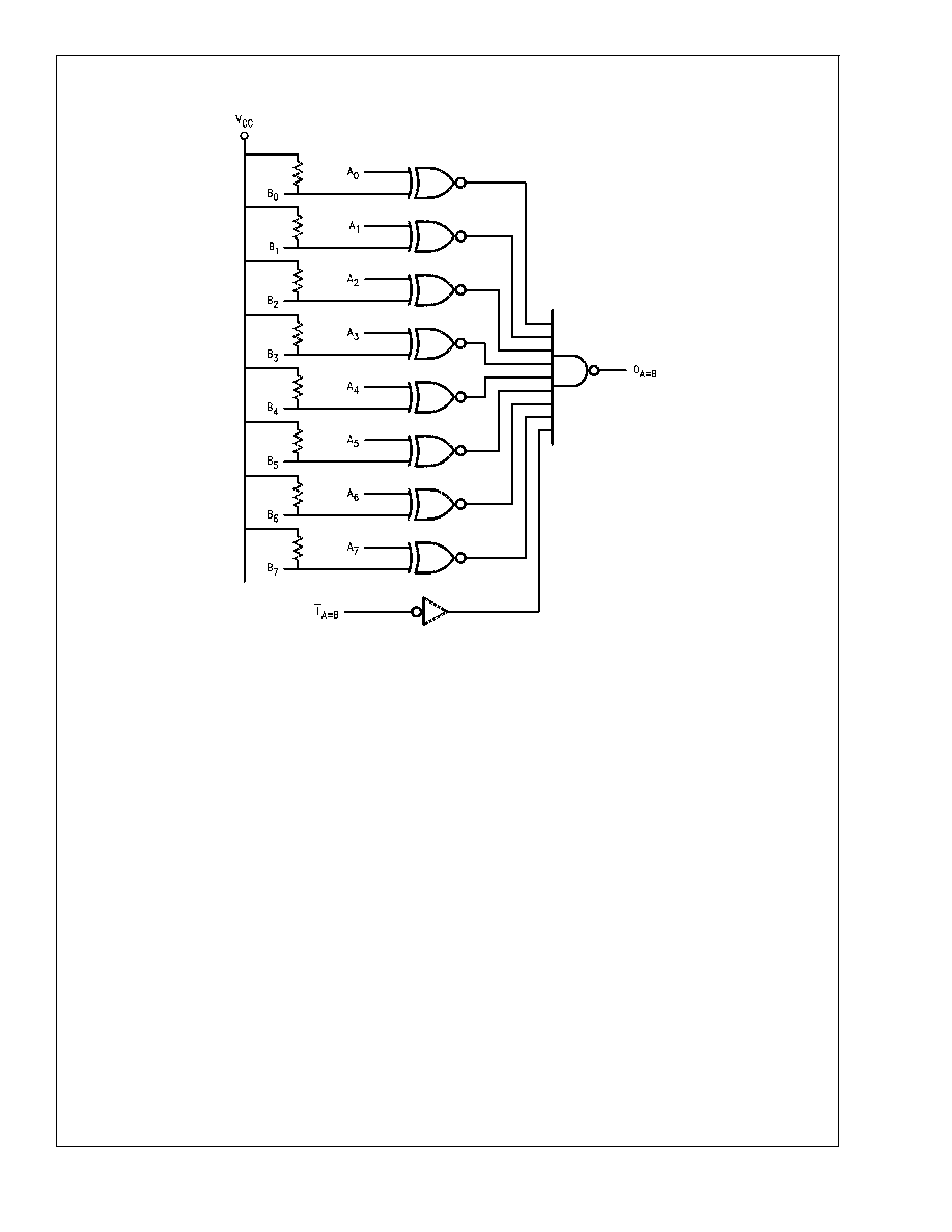
Logic Diagram
DS100234-5
Please note that this diagram is provided only for the understanding of logic operations and should not be used to estimate propagation delays.
54AC520
∑
54ACT520
www.national.com
3
Absolute Maximum Ratings
(Note 1)
If Military/Aerospace specified devices are required,
please contact the National Semiconductor Sales Office/
Distributors for availability and specifications.
Supply Voltage (V
CC
)
-0.5V to +7.0V
DC Input Diode Current (I
IK
)
V
I
= -0.5V
-20 mA
V
I
= V
CC
+ 0.5V
+20 mA
DC Input Voltage (V
I
)
-0.5V to V
CC
+ 0.5V
DC Output Diode Current (I
OK
)
V
O
= -0.5V
-20 mA
V
O
= V
CC
+ 0.5V
+20 mA
DC Output Voltage (V
O
)
-0.5V to V
CC
+ 0.5V
DC Output Source
or Sink Current (I
O
)
±
50 mA
DC V
CC
or Ground Current
per Output Pin (I
CC
or I
GND
)
±
50 mA
Storage Temperature (T
STG
)
-65∞C to +150∞C
Junction Temperature (T
J
)
CDIP
175∞C
Recommended Operating
Conditions
Supply Voltage (V
CC
)
'AC
2.0V to 6.0V
'ACT
4.5V to 5.5V
Input Voltage (V
I
)
0V to V
CC
Output Voltage (V
O
)
0V to V
CC
Operating Temperature (T
A
)
54AC/ACT
-55∞C to +125∞C
Minimum Input Edge Rate (
V/
t)
'AC Devices
V
IN
from 30% to 70% of V
CC
V
CC
@
3.3V, 4.5V, 5.5V
125 mV/ns
Minimum Input Edge Rate (
V/
t)
'ACT Devices
V
IN
from 0.8V to 2.0V
V
CC
@
4.5V, 5.5V
125 mV/ns
Note 1: Absolute maximum ratings are those values beyond which damage
to the device may occur. The databook specifications should be met, without
exception, to ensure that the system design is reliable over its power supply,
temperature, and output/input loading variables. National does not recom-
mend operation of FACT
TM
circuits outside databook specifications.
DC Characteristics for 'AC Family Devices
54AC
Symbol
Parameter
V
CC
T
A
=
Units
Conditions
(V)
-55∞C to +125∞C
Guaranteed Limits
V
IH
Minimum High Level
3.0
2.1
V
OUT
= 0.1V
Input Voltage
4.5
3.15
V
or V
CC
- 0.1V
5.5
3.85
V
IL
Maximum Low Level
3.0
0.9
V
OUT
= 0.1V
Input Voltage
4.5
1.35
V
or V
CC
- 0.1V
5.5
1.65
V
OH
Minimum High Level
3.0
2.9
I
OUT
= -50 µA
Output Voltage
4.5
4.4
V
5.5
5.4
(Note 2)
V
IN
= V
IL
or V
IH
3.0
2.4
I
OH
= -12 mA
4.5
3.7
V
I
OH
= -24 mA
5.5
4.7
I
OH
= -24 mA
V
OL
Maximum Low Level
3.0
0.1
I
OUT
= 50 µA
Output Voltage
4.5
0.1
V
5.5
0.1
(Note 2)
V
IN
= V
IL
or V
IH
3.0
0.50
I
OL
= 12 mA
4.5
0.50
V
I
OL
= 24 mA
5.5
0.50
I
OL
= 24 mA
I
IN
Maximum Input
5.5
±
1.0
µA
V
I
= V
CC
, GND
Leakage Current
A Inputs Only
I
IH
Maximum Input
5.5
20.0
µA
V
I
= V
CC
High Leakage Current
B Inputs Only
54AC520
∑
54ACT520
www.national.com
4

DC Characteristics for 'AC Family Devices
(Continued)
54AC
Symbol
Parameter
V
CC
T
A
=
Units
Conditions
(V)
-55∞C to +125∞C
Guaranteed Limits
I
IL
Maximum Input
5.5
-1.5
mA
V
I
= V
CC
Low Leakage Current
B Inputs Only
I
OLD
Minimum Dynamic
(Note 3)
5.5
50
mA
V
OLD
= 1.65V Max
I
OHD
Output Current
5.5
-50
mA
V
OHD
= 3.85V Min
I
CC
Maximum Quiescent
5.5
80.0
µA
V
IN
= V
CC
Supply Current
I
CC
Maximum Quiescent
5.5
8.0
mA
V
IN
= GND
Supply Current
Note 2: All outputs loaded; thresholds on input associated with output under test.
Note 3: Maximum test duration 2.0 ms, one output loaded at a time.
DC Characteristics for 'ACT Family Devices
54ACT
Symbol
Parameter
V
CC
T
A
=
Units
Conditions
(V)
-55∞C to +125∞C
Guaranteed Limits
V
IH
Minimum High Level
4.5
2.0
V
V
OUT
= 0.1V
Input Voltage
5.5
2.0
or V
CC
- 0.1V
V
IL
Maximum Low Level
4.5
0.8
V
V
OUT
= 0.1V
Input Voltage
5.5
0.8
or V
CC
- 0.1V
V
OH
Minimum High Level
4.5
4.4
V
I
OUT
= -50 µA
Output Voltage
5.5
5.4
(Note 4)
V
IN
= V
IL
or V
IH
4.5
3.70
V
I
OH
= -24 mA
5.5
4.70
I
OH
= -24 mA
V
OL
Maximum Low Level
4.5
0.1
V
I
OUT
= 50 µA
Output Voltage
5.5
0.1
(Note 4)
V
IN
= V
IL
or V
IH
4.5
0.50
V
I
OL
= 24 mA
5.5
0.50
I
OL
= 24 mA
I
IN
Maximum Input
5.5
±
1.0
µA
V
I
= V
CC
, GND
Leakage Current
I
IH
Maximum Input
5.5
10.0
µA
V
I
= V
CC
High Leakage Current
B Inputs Only
I
IL
Maximum Input
5.5
-1.0
mA
V
I
= V
CC
Low Leakage Current
B Inputs Only
I
CCT
Maximum
5.5
1.6
mA
V
I
= V
CC
- 2.1V
I
CC
/Input
I
OLD
Minimum Dynamic
(Note 5)
5.5
50
mA
V
OLD
= 1.65V Max
I
OHD
Output Current
5.5
-50
mA
V
OHD
= 3.85V Min
I
CC
Maximum Quiescent
5.5
80.0
µA
V
IN
= V
CC
Supply Current
or GND
54AC520
∑
54ACT520
www.national.com
5