
54ACQ374
∑
54ACTQ374
Quiet Series Octal D Flip-Flop with TRI-STATE
Æ
Outputs
General Description
The 'ACQ/'ACTQ374 is a high-speed, low-power octal
D-type flip-flop featuring separate D-type inputs for each
flip-flop and TRI-STATE outputs for bus-oriented applica-
tions. A buffered Clock (CP) and Output Enable (OE) are
common to all flip-flops.
The 'ACQ/'ACTQ374 utilizes Quiet Series technology to
guarantee quiet output switching and improve dynamic
threshold performance. FACT Quiet Series
TM
features
GTO
TM
output control and undershoot corrector in addition to
a split ground bus for superior performance.
Features
n
I
CC
and I
OZ
reduced by 50%
n
Guaranteed simultaneous switching noise level and
dynamic threshold performance
n
Improved latch-up immunity
n
Buffered positive edge-triggered clock
n
TRI-STATE outputs drive bus lines or buffer memory
address registers
n
Outputs source/sink 24 mA
n
Faster prop delays than the standard 'AC/'ACT374
n
4 kV minimum ESD immunity
n
Standard Military Drawing (SMD)
-- 'ACTQ374: 5962-92189
-- 'ACQ374: 5962-92179
Logic Symbols
Connection Diagrams
GTO
TM
is a trademark of National Semiconductor Corporation.
TRI-STATE
Æ
is a registered trademark of National Semiconductor Corporation.
FACT
Æ
is a registered trademark of Fairchild Semiconductor Corporation.
FACT Quiet Series
TM
is a trademark of Fairchild Semiconductor Corporation.
DS100239-1
IEEE/IEC
DS100239-2
Pin Assignment for DIP
and Flatpak
DS100239-3
Pin Assignment for LCC
DS100239-4
August 1998
54ACQ374
∑
54ACTQ374
Quiet
Series
Octal
D
Flip-Flop
with
TRI-ST
A
T
E
Outputs
© 1998 National Semiconductor Corporation
DS100239
www.national.com

Connection Diagrams
(Continued)
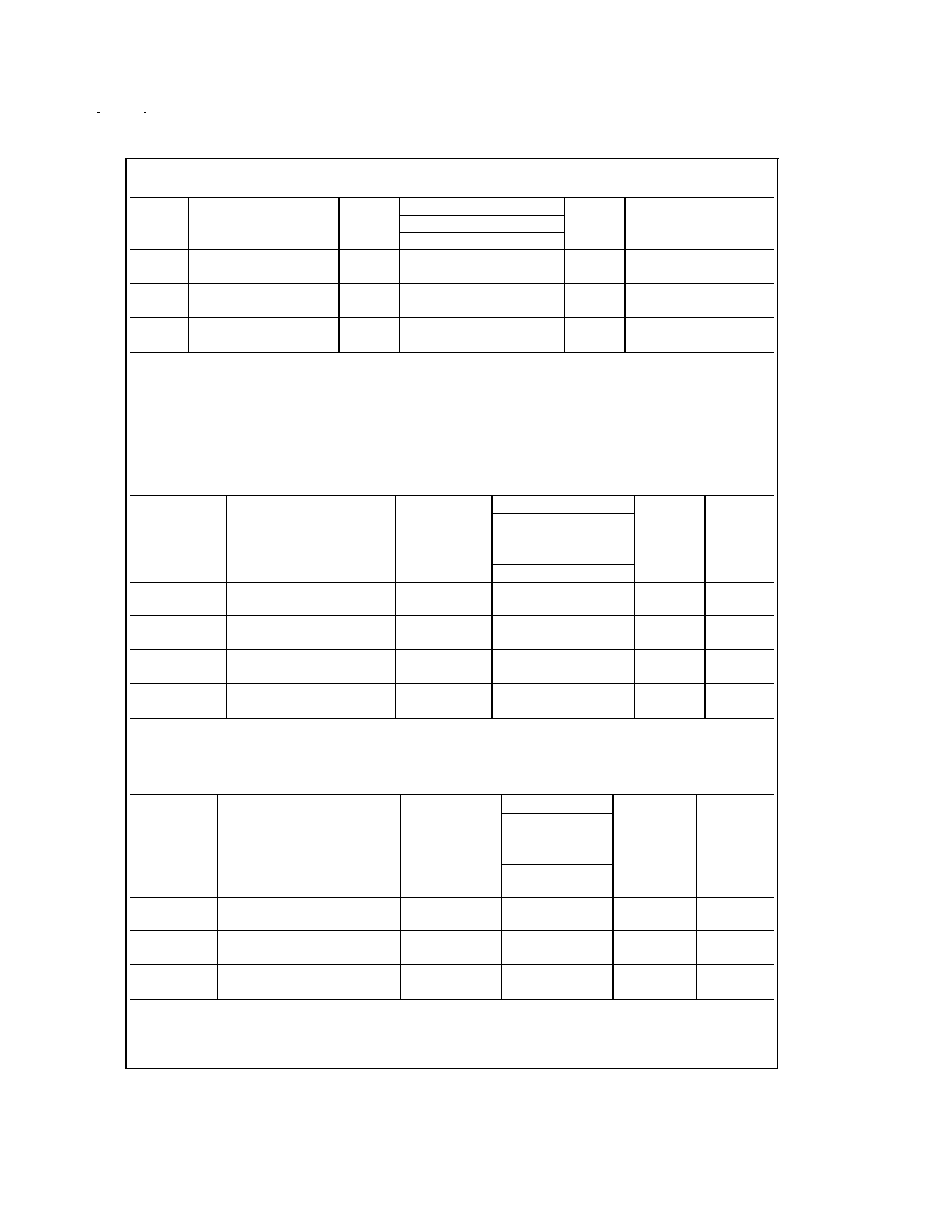
Pin Names
Description
D
0
≠D
7
Data Inputs
CP
Clock Pulse Input
OE
TRI-STATE Output Enable Input
O
0
≠O
7
TRI-STATE Outputs
Functional Description
The 'ACQ/'ACTQ374 consists of eight edge-triggered
flip-flops with individual D-type inputs and TRI-STATE true
outputs. The buffered clock and buffered Output Enable are
common to all flip-flops. The eight flip-flops will store the
state of their individual D inputs that meet the setup and hold
time requirements on the LOW-to-HIGH Clock (CP) transi-
tion. With the Output Enable (OE) LOW, the contents of the
eight flip-flops are available at the outputs. When the OE is
HIGH, the outputs go to the high impedance state. Operation
of the OE input does not affect the state of the flip-flops.
Truth Table
Inputs
Outputs
D
n
CP
OE
O
n
H
N
L
H
L
N
L
L
X
X
H
Z
H = HIGH Voltage Level
L = LOW Voltage Level
X = Immaterial
Z = High Impedance
N
= LOW-to-HIGH Transition
Logic Diagram
DS100239-5
Please note that this diagram is provided only for the understanding of logic operations and should not be used to estimate propagation delays.
www.national.com
2
Absolute Maximum Ratings
(Note 1)
If Military/Aerospace specified devices are required,
please contact the National Semiconductor Sales Office/
Distributors for availability and specifications.
Supply Voltage (V
CC
)
-0.5V to +7.0V
DC Input Diode Current (I
IK
)
V
I
= -0.5V
-20 mA
V
I
= V
CC
+ 0.5V
+20 mA
DC Input Voltage (V
I
)
-0.5V to V
CC
+ 0.5V
DC Output Diode Current (I
OK
)
V
O
= -0.5V
-20 mA
V
O
= V
CC
+ 0.5V
+20 mA
DC Output Voltage (V
O
)
-0.5V to V
CC
+ 0.5V
DC Output Source
or Sink Current (I
O
)
±
50 mA
DC V
CC
or Ground Current
per Output Pin (I
CC
or I
GND
)
±
50 mA
Storage Temperature (T
STG
)
-65∞C to +150∞C
DC Latch-Up Source or Sink Current
±
300 mA
Junction Temperature (T
J
)
CDIP
175∞C
Recommended Operating
Conditions
Supply Voltage (V
CC
)
'ACQ
2.0V to 6.0V
'ACTQ
4.5V to 5.5V
Input Voltage (V
I
)
0V to V
CC
Output Voltage (V
O
)
0V to V
CC
Operating Temperature (T
A
)
54ACQ/ACTQ
-55∞C to +125∞C
Minimum Input Edge Rate
V/
t
'ACQ Devices
V
IN
from 30% to 70% of V
CC
V
CC
@
3.0V, 4.5V, 5.5V
125 mV/ns
Minimum Input Edge Rate
V/
t
'ACTQ devices
V
IN
from 0.8V to 2.0V
V
CC
@
4.5V, 5.5V
125 mV/ns
Note 1: Absolute maximum ratings are those values beyond which damage
to the device may occur. The databook specifications should be met, without
exception, to ensure that the system design is reliable over its power supply,
temperature, and output/input loading variables. National does not recom-
mend operation of FACT
Æ
circuits outside databook specifications.
Note 2: All commercial packaging is not recommended for applications re-
quiring greater than 2000 temperature cycles from -40∞C to +125∞C.
DC Characteristics for 'ACQ Family Devices
54ACQ
Symbol
Parameter
V
CC
T
A
= -55∞C to +125∞C
Units
Conditions
(V)
Guaranteed Limits
V
IH
Minimum High Level
3.0
2.1
V
OUT
= 0.1V
Input Voltage
4.5
3.15
V
or V
CC
- 0.1V
5.5
3.85
V
IL
Maximum Low Level
3.0
0.9
V
OUT
= 0.1V
Input Voltage
4.5
1.35
V
or V
CC
- 0.1V
5.5
1.65
V
OH
Minimum High Level
3.0
2.9
I
OUT
= -50 µA
Output Voltage
4.5
4.4
V
5.5
5.4
(Note 3)
V
IN
= V
IL
or V
IH
3.0
2.4
I
OH
= -12 mA
4.5
3.7
V
I
OH
= -24 mA
5.5
4.7
I
OH
= -24 mA
V
OL
Maximum Low Level
3.0
0.1
I
OUT
= 50 µA
Output Voltage
4.5
0.1
V
5.5
0.1
(Note 3)
3.0
0.50
I
OL
= 12 mA
4.5
0.50
V
I
OL
= 24 mA
5.5
0.50
I
OL
= 24 mA
I
IN
Maximum Input
5.5
±
1.0
µA
V
I
= V
CC
, GND
Leakage Current
(Note 5)
(Note 4)
Minimum Dynamic
Output Current
I
OLD
5.5
50
mA
V
OLD
= 1.65V Max
I
OHD
5.5
-50
mA
V
OHD
= 3.85V Min
www.national.com
3

DC Characteristics for 'ACQ Family Devices
(Continued)
54ACQ
Symbol
Parameter
V
CC
T
A
= -55∞C to +125∞C
Units
Conditions
(V)
Guaranteed Limits
I
CC
Maximum Quiescent
5.5
80.0
µA
V
IN
= V
CC
Supply Current
or GND (Note 5)
I
OZ
Maximum TRI-STATE
V
I
(OE) = V
IL
, V
IH
Leakage Current
5.5
±
5.0
µA
V
I
= V
CC
, GND
V
O
= V
CC
, GND
V
OLP
Quiet Output
5.0
1.5
V
Maximum Dynamic V
OL
(Notes 6, 7)
V
OLV
Quiet Output
5.0
-1.2
V
Minimum Dynamic V
OL
(Notes 6, 7)
Note 3: All outputs loaded; thresholds on input associated with output under test.
Note 4: Maximum test duration 2.0 ms, one output loaded at a time.
Note 5: I
IN
and I
CC
@
3.0V are guaranteed to be less than or equal to the respective limit
@
5.5V V
CC
.
I
CC
for 54ACQ
@
25∞C is identical to 74ACQ
@
25∞C.
Note 6: Plastic DIP Package.
Note 7: Max number of outputs defined as (n). Data inputs are driven 0V to 5V. One output
@
GND.
Note 8: Max number of data inputs (n) switching. (n-1) inputs switching 0V to 5V ('ACQ). Input-under-test switching: 5V to threshold (V
ILD
), 0V to threshold (V
IHD
),
f = 1 MHz.
DC Characteristics for 'ACTQ Family Devices
54ACTQ
Symbol
Parameter
V
CC
T
A
= -55∞C to +125∞C
Units
Conditions
(V)
Guaranteed Limits
V
IH
Minimum High Level
4.5
2.0
V
V
OUT
= 0.1V
Input Voltage
5.5
2.0
or V
CC
- 0.1V
V
IL
Maximum Low Level
4.5
0.8
V
V
OUT
= 0.1V
Input Voltage
5.5
0.8
or V
CC
- 0.1V
V
OH
Minimum High Level
4.5
4.4
V
I
OUT
= -50 µA
Output Voltage
5.5
5.4
(Note 9)
V
IN
= V
IL
or V
IH
4.5
3.70
V
I
OH
= -24 mA
5.5
4.70
I
OH
= -24 mA
V
OL
Maximum Low Level
4.5
0.1
V
I
OUT
= 50 µA
Output Voltage
5.5
0.1
(Note 9)
V
IN
= V
IL
or V
IH
4.5
0.50
V
I
OL
= 24 mA
5.5
0.50
I
OL
= 24 mA
I
IN
Maximum Input
5.5
±
1.0
µA
V
I
= V
CC
, GND
Leakage Current
I
OZ
Maximum TRI-STATE
5.5
±
5.0
µA
V
I
= V
IL
, V
IH
Current
V
O
= V
CC
, GND
I
CCT
Maximum I
CC
/Input
5.5
1.6
mA
V
I
= V
CC
- 2.1V
(Note 9)
I
OLD
Minimum Dynamic
Output Current
5.5
50
mA
V
OLD
= 1.65V Max
I
OHD
5.5
-50
mA
V
OHD
= 3.85V Min
www.national.com
4
DC Characteristics for 'ACTQ Family Devices
(Continued)
54ACTQ
Symbol
Parameter
V
CC
T
A
= -55∞C to +125∞C
Units
Conditions
(V)
Guaranteed Limits
I
CC
Maximum Quiescent
5.5
80.0
µA
V
IN
= V
CC
Supply Current
or GND (Note 11)
V
OLP
Quiet Output
5.0
1.5
V
Maximum Dynamic V
OL
(Notes 12, 13)
V
OLV
Quiet Output
5.0
-1.2
V
Minimum Dynamic V
OL
(Notes 12, 13)
Note 9: All outputs loaded; thresholds on input associated with output under test.
Note 10: Maximum test duration 2.0 ms, one output loaded at a time.
Note 11: I
CC
for 54ACTQ
@
25∞C is identical to 74ACTQ
@
25∞C.
Note 12: Plastic DIP package.
Note 13: Max number of outputs defined as (n). Data inputs are driven 0V to 3V. One output
@
GND
Note 14: Max number of data inputs (n) switching. (n-1) inputs switching 0V to 3V ('ACTQ). Input-under-test switching: 3V to threshold (V
ILD
), 0V to threshold (V
IHD
),
f = 1 MHz.
AC Electrical Characteristics
54ACQ
V
CC
T
A
= -55∞C
Fig.
Symbol
Parameter
(V)
to +125∞C
Units
No.
(Note 15)
C
L
= 50 pF
Min
Max
f
max
Maximum Clock
3.3
95
MHz
Frequency
5.0
95
t
PLH
, t
PHL
Propagation Delay
3.3
1.0
16.5
ns
CP to O
n
5.0
1.0
11.0
t
PZL
, t
PZH
Output Enable Time
3.3
1.0
16.5
ns
5.0
1.0
11.5
t
PHZ
, t
PLZ
Output Disable Time
3.3
1.0
12.0
ns
5.0
1.0
10.5
Note 15: Voltage Range 5.0 is 5.0V
±
0.5V
Voltage Range 3.3 is 3.3V
±
0.3V
AC Operating Requirements
54ACQ
V
CC
T
A
= -55∞C
Fig.
Symbol
Parameter
(V)
to +125∞C
Units
No.
(Note 16)
C
L
= 50 pF
Guaranteed
Minimum
t
s
Setup Time, HIGH or LOW
3.3
3.0
ns
D
n
to CP
5.0
3.0
t
h
Hold Time, HIGH or LOW
3.3
2.0
ns
D
n
to CP
5.0
1.5
t
w
CP Pulse Width,
3.3
5.0
ns
HIGH or LOW
5.0
5.0
Note 16: Voltage Range 5.0 is 5.0V
±
0.5V
Voltage Range 3.3 is 3.3V
±
0.3V
www.national.com
5