
TL F 10231
54AC74AC378
Parallel
D
Register
with
Enable
March 1993
54AC 74AC378
Parallel D Register with Enable
General Description
The 'AC378 is a 6-bit register with a buffered common En-
able This device is similar to the 'AC174 but with common
Enable rather than common Master Reset
Features
Y
6-bit high-speed parallel register
Y
Positive edge-triggered D-type inputs
Y
Fully buffered common clock and enable inputs
Y
Input clamp diodes limit high-speed termination effects
Y
Standard Military Drawing (SMD)
'AC378 5962-91605
Logic Symbols
Connection Diagrams
TL F 10231 ≠ 1
IEEE IEC
TL F 10231 ≠ 4
Pin Assignment for
DIP SOIC and Flatpak
TL F 10231 ≠ 2
Pin Assignment
for LCC
TL F 10231 ≠ 3
Pin Names
Description
E
Enable Input (Active LOW)
D
0
≠ D
5
Data Inputs
CP
Clock Pulse Input (Active Rising Edge)
Q
0
≠ Q
5
Outputs
FACT
TM
is a trademark of National Semiconductor Corporation
C1995 National Semiconductor Corporation
RRD-B30M75 Printed in U S A

Functional Description
The 'AC378 consists of six edge-triggered D-type flip-flops
with individual D inputs and Q inputs The Clock (CP) and
Enable (E) inputs are common to all flip-flops
When the E input is LOW new data is entered into the
register on the LOW-to-HIGH transition of the CP input
When the E input is HIGH the register will retain the present
data independent of the CP input
Truth Table
Inputs
Output
E
CP
D
n
Q
n
H
L
X
No Change
L
L
H
H
L
L
L
L
H
e
HIGH Voltage Level
L
e
LOW Voltage Level
X
e
Immaterial
L
e
LOW-to-HIGH Clock Transition
Logic Diagram
TL F 10231 ≠ 5
Please note that this diagram is provided only for the understanding of logic operations and should not be used to estimate propagation delays
2

Absolute Maximum Ratings
(Note 1)
If Military Aerospace specified devices are required
please contact the National Semiconductor Sales
Office Distributors for availability and specifications
Supply Voltage (V
CC
)
b
0 5V to
a
7 0V
DC Input Diode Current (I
IK
)
V
I
e b
0 5V
b
20 mA
V
I
e
V
CC
a
0 5V
a
20 mA
DC Input Voltage (V
I
)
b
0 5V to V
CC
a
0 5V
DC Output Diode Current (I
OK
)
V
O
e b
0 5V
b
20 mA
V
O
e
V
CC
a
0 5V
a
20 mA
DC Output Voltage (V
O
)
b
0 5V to V
CC
a
0 5V
DC Output Source
or Sink Current (I
O
)
g
50 mA
DC V
CC
or Ground Current
per Output Pin (I
CC
or I
GND
)
g
50 mA
Storage Temperature (T
STG
)
b
65 C to
a
150 C
Junction Temperature (T
J
)
CDIP
175 C
PDIP
140 C
Note 1
Absolute maximum ratings are those values beyond which damage
to the device may occur The databook specifications should be met without
exception to ensure that the system design is reliable over its power supply
temperature and output input loading variables National does not recom-
mend operation of FACT
TM
circuits outside databook specifications
Recommended Operating
Conditions
Supply Voltage (V
CC
)
'AC
2 0V to 6 0V
Input Voltage (V
I
)
0V to V
CC
Output Voltage (V
O
)
0V to V
CC
Operating Temperature (T
A
)
74AC
b
40 C to
a
85 C
54AC
b
55 C to
a
125 C
Minimum Input Edge Rate (DV Dt)
'AC Devices
V
IN
from 30% to 70% of V
CC
V
CC
3 3V 4 5V 5 5V
125 mV ns
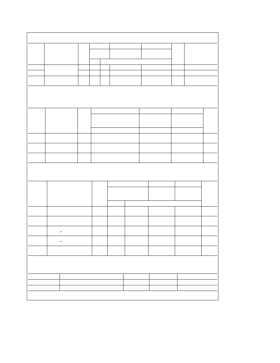
DC Characteristics for 'AC Family Devices
74AC
54AC
74AC
Symbol
Parameter
V
CC
T
A
e a
25 C
T
A
e
T
A
e
Units
Conditions
(V)
b
55 C to
a
125 C
b
40 C to
a
85 C
Typ
Guaranteed Limits
V
IH
Minimum High Level
3 0
1 5
2 1
2 1
2 1
V
OUT
e
0 1V
Input Voltage
4 5
2 25
3 15
3 15
3 15
V
or V
CC
b
0 1V
5 5
2 75
3 85
3 85
3 85
V
IL
Maximum Low Level
3 0
1 5
0 9
0 9
0 9
V
OUT
e
0 1V
Input Voltage
4 5
2 25
1 35
1 35
1 35
V
or V
CC
b
0 1V
5 5
2 75
1 65
1 65
1 65
V
OH
Minimum High Level
3 0
2 99
2 9
2 9
2 9
I
OUT
e b
50 mA
Output Voltage
4 5
4 49
4 4
4 4
4 4
V
5 5
5 49
5 4
5 4
5 4
V
IN
e
V
IL
or V
IH
3 0
2 56
2 4
2 46
b
12 mA
4 5
3 86
3 7
3 76
V
I
OH
b
24 mA
5 5
4 86
4 7
4 76
b
24 mA
V
OL
Maximum Low Level
3 0
0 002
0 1
0 1
0 1
I
OUT
e
50 mA
Output Voltage
4 5
0 001
0 1
0 1
0 1
V
5 5
0 001
0 1
0 1
0 1
V
IN
e
V
IL
or V
IH
3 0
0 36
0 5
0 44
12 mA
4 5
0 36
0 5
0 44
V
I
OL
24 mA
5 5
0 36
0 5
0 44
24 mA
I
IN
Maximum Input
5 5
g
0 1
g
1 0
g
1 0
m
A
V
I
e
V
CC
GND
Leakage Current
All outputs loaded thresholds on input associated with output under test
3
DC Characteristics for 'AC Family Devices
(Continued)
74AC
54AC
74AC
Symbol
Parameter
V
CC
T
A
e
T
A
e
T
A
e
Units
Conditions
(V)
a
25 C
b
55 C to
a
125 C
b
40 C to
a
85 C
Typ
Guaranteed Limits
I
OLD
Minimum Dynamic
5 5
50
75
mA
V
OLD
e
1 65V Max
I
OHD
Output Current
5 5
b
50
b
75
mA
V
OHD
e
3 85V Min
I
CC
Maximum Quiescent
5 5
4 0
80 0
40 0
m
A
V
IN
e
V
CC
Supply Current
or GND
Maximum test duration 2 0 ms one output loaded at a time
Note
I
IN
and I
CC
3 0V are guaranteed to be less than or equal to the respective limit
5 5V V
CC
I
CC
for 54AC
25 C is identical to 74AC
25 C
AC Electrical Characteristics
74AC
54AC
74AC
V
CC
T
A
e a
25 C
T
A
e b
55 C
T
A
e b
40 C
Symbol
Parameter
(V)
C
L
e
50 pF
to
a
125 C
to
a
85 C
Units
C
L
e
50 pF
C
L
e
50 pF
Min
Typ
Max
Min
Max
Min
Max
f
max
Maximum Clock
3 3
125
160
95
110
MHz
Frequency
5 0
160
200
95
145
t
PLH
Propagation Delay
3 3
2 5
8 5
11 0
1 5
12 0
2 5
12 5
ns
CP to Q
n
5 0
1 5
6 0
8 0
1 5
9 0
1 5
9 0
t
PHL
Propagation Delay
3 3
2 5
8 0
10 5
1 5
12 0
2 5
11 0
ns
CP to Q
n
5 0
1 5
5 5
7 5
1 5
9 0
1 5
8 0
Voltage Range 3 3 is 3 3V
g
0 3V
Voltage Range 5 0 is 5 0V
g
0 5V
AC Operating Requirements
74AC
54AC
74AC
V
CC
T
A
e a
25 C
T
A
e b
55 C
T
A
e b
40 C
Symbol
Parameter
(V)
C
L
e
50 pF
to
a
125 C
to
a
85 C
Units
C
L
e
50 pF
C
L
e
50 pF
Typ
Guaranteed Minimum
t
s
Setup Time HIGH or LOW
3 3
1 5
3 0
4 0
3 5
ns
D
n
to CP
5 0
1 0
2 0
4 0
2 5
t
h
Hold Time HIGH or LOW
3 3
1 0
2 0
4 0
2 0
ns
D
n
to CP
5 0
1 0
2 0
4 0
2 0
t
s
Setup Time HIGH or
3 3
0
2 0
2 5
2 0
ns
LOW E to CP
5 0
0
2 0
2 5
2 0
t
h
Hold Time HIGH or
3 3
1 0
2 0
4 0
2 0
ns
LOW E to CP
5 0
1 0
2 0
4 0
2 0
t
w
CP Pulse Width
3 3
3 0
4 5
6 5
5 5
ns
HIGH or LOW
5 0
2 0
3 5
6 5
4 0
Voltage Range 3 3 is 3 3V
g
0 3V
Voltage Range 5 0 is 5 0V
g
0 5V
Capacitance
Symbol
Parameter
Typ
Units
Conditions
C
IN
Input Capacitance
4 5
pF
V
CC
e
OPEN
C
PD
Power Dissipation Capacitance
28
pF
V
CC
e
5 0V
4

Ordering Information
The device number is used to form part of a simplified purchasing code where a package type and temperature range are
defined as follows
74AC
378
P
C
QR
Temperature Range Family
Special Variations
74AC
e
Commercial
X
e
Devices shipped in 13 reels
54AC
e
Military
QR
e
Commercial grade device with
burn-in
Device Type
QB
e
Military grade with environmental
and burn-in processing shipped
Package Code
in tubes
P
e
Plastic DIP
D
e
Ceramic DIP
Temperature Range
F
e
Flatpak
C
e
Commercial (
b
40 C to
a
85 C)
L
e
Leadless Ceramic Chip Carrier (LCC)
M
e
Military (
b
55 C to
a
125 C)
S
e
Small Outline (SOIC)
5