
TL F 9498
54F74F194
4-Bit
Bidirectional
Universal
Shift
Register
November 1994
54F 74F194
4-Bit Bidirectional Universal Shift Register
General Description
The 'F194 is a high-speed 4-bit bidirectional universal shift
register As a high-speed multifunctional sequential build-
ing block it is useful in a wide variety of applications It may
be used in serial-serial shift left shift right serial-parallel
parallel-serial and parallel-parallel data register transfers
The 'F194 is similar in operation to the 'F195 universal shift
register with added features of shift left without external
connections and hold (do nothing) modes of operation
Features
Y
Typical shift frequency of 150 MHz
Y
Asynchronous master reset
Y
Hold (do nothing) mode
Y
Fully synchronous serial or parallel data transfers
Commercial
Military
Package
Package Description
Number
74F194PC
N16E
16-Lead (0 300 Wide) Molded Dual-In-Line
54F194DM (Note 2)
J16A
16-Lead Ceramic Dual-In-Line
74F194SC (Note 1)
M16A
16-Lead (0 150 Wide) Molded Small Outline JEDEC
74F194SJ (Note 1)
M16D
16-Lead (0 300 Wide) Molded Small Outline EIAJ
54F194FM (Note 2)
W16A
16-Lead Cerpack
54F194LM (Note 2)
E20A
20-Lead Ceramic Leadless Chip Carrier Type C
Note 1
Devices also available in 13
reel Use suffix
e
SCX and SJX
Note 2
Military grade device with environmental and burn-in processing Use suffix
e
DMQB FMQB and LMQB
Logic Symbols
Connection Diagrams
IEEE IEC
TL F 9498 � 5
TL F 9498 � 3
Pin Assignment for
DIP SOIC and Flatpak
TL F 9498 � 1
Pin Assignment
for LCC
TL F 9498 � 2
TRI-STATE
is a registered trademark of National Semiconductor Corporation
C1995 National Semiconductor Corporation
RRD-B30M105 Printed in U S A

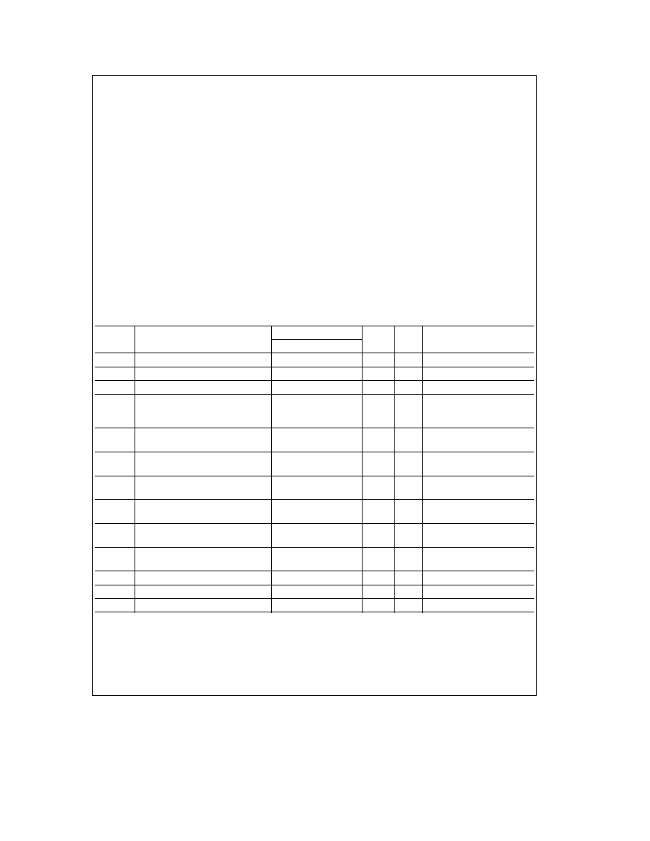
Unit Loading Fan Out
Pin
54F 74F
Names
Description
U L
Input I
IH
I
IL
HIGH LOW
Output I
OH
I
OL
S
0
S
1
Mode Control Inputs
1 0 1 0
20 mA
b
0 6 mA
P
0
� P
3
Parallel Data Inputs
1 0 1 0
20 mA
b
0 6 mA
D
SR
Serial Data Input (Shift Right)
1 0 1 0
20 mA
b
0 6 mA
D
SL
Serial Data Input (Shift Left)
1 0 1 0
20 mA
b
0 6 mA
CP
Clock Pulse Input (Active Rising Edge)
1 0 1 0
20 mA
b
0 6 mA
MR
Asynchronous Master Reset Input (Active LOW)
1 0 1 0
20 mA
b
0 6 mA
Q
0
� Q
3
Parallel Outputs
50 33 3
b
1 mA 20 mA
Functional Description
The 'F194 contains four edge-triggered D flip-flops and the
necessary interstage logic to synchronously perform shift
right shift left parallel load and hold operations Signals
applied to the Select (S
0
S
1
) inputs determine the type of
operation as shown in the Mode Select Table Signals on
the Select Parallel data (P
0
� P
3
) and Serial data (D
SR
D
SL
)
inputs can change when the clock is in either state provid-
ed only that the recommended setup and hold times with
respect to the clock rising edge are observed A LOW sig-
nal on Master Reset (MR) overrides all other inputs and
forces the outputs LOW
Mode Select Table
Operating
Inputs
Outputs
Mode
MR
S
1
S
0
D
SR
D
SL
P
n
Q
0
Q
1
Q
2
Q
3
Reset
L
X
X
X
X
X
L
L
L
L
Hold
H
l
l
X
X
X
q
0
q
1
q
2
q
3
Shift Left
H
h
l
X
l
X
q
1
q
2
q
3
L
H
h
l
X
h
X
q
1
q
2
q
3
H
Shift Right
H
l
h
l
X
X
L
q
0
q
1
q
2
H
l
h
h
X
X
H
q
0
q
1
q
2
Parallel Load
H
h
h
X
X
p
n
p
0
p
1
p
2
p
3
H (h)
e
High Voltage Level
L (l)
e
Low Voltage Level
p
n
(q
n
)
e
Lower case letters indicate the state of the referenced input (or output) one setup time prior to the LOW-to-HIGH clock transition
X
e
Immaterial
Logic Diagram
TL F 9498 � 4
Please note that this diagram is provided only for the understanding of logic operations and should not be used to estimate propagation delays
2
Absolute Maximum Ratings
(Note 1)
If Military Aerospace specified devices are required
please contact the National Semiconductor Sales
Office Distributors for availability and specifications
Storage Temperature
b
65 C to
a
150 C
Ambient Temperature under Bias
b
55 C to
a
125 C
Junction Temperature under Bias
b
55 C to
a
175 C
Plastic
b
55 C to
a
150 C
V
CC
Pin Potential to
Ground Pin
b
0 5V to
a
7 0V
Input Voltage (Note 2)
b
0 5V to
a
7 0V
Input Current (Note 2)
b
30 mA to
a
5 0 mA
Voltage Applied to Output
in HIGH State (with V
CC
e
0V)
Standard Output
b
0 5V to V
CC
TRI-STATE Output
b
0 5V to
a
5 5V
Current Applied to Output
in LOW State (Max)
twice the rated I
OL
(mA)
Note 1
Absolute maximum ratings are values beyond which the device may
be damaged or have its useful life impaired Functional operation under
these conditions is not implied
Note 2
Either voltage limit or current limit is sufficient to protect inputs
Recommended Operating
Conditions
Free Air Ambient Temperature
Military
b
55 C to
a
125 C
Commercial
0 C to
a
70 C
Supply Voltage
Military
a
4 5V to
a
5 5V
Commercial
a
4 5V to
a
5 5V
DC Electrical Characteristics
Symbol
Parameter
54F 74F
Units
V
CC
Conditions
Min
Typ
Max
V
IH
Input HIGH Voltage
2 0
V
Recognized as a HIGH Signal
V
IL
Input LOW Voltage
0 8
V
Recognized as a LOW Signal
V
CD
Input Clamp Diode Voltage
b
1 2
V
Min
I
IN
e b
18 mA
V
OH
Output HIGH
54F 10% V
CC
2 5
I
OH
e b
1 mA
Voltage
74F 10% V
CC
2 5
V
Min
I
OH
e b
1 mA
74F 5% V
CC
2 7
I
OH
e b
1 mA
V
OL
Output LOW
54F 10% V
CC
0 5
V
Min
I
OL
e
20 mA
Voltage
74F 10% V
CC
0 5
I
OL
e
20 mA
I
IH
Input HIGH
54F
20 0
m
A
Max
V
IN
e
2 7V
Current
74F
5 0
I
BVI
Input HIGH Current
54F
100
m
A
Max
V
IN
e
7 0V
Breakdown Test
74F
7 0
I
CEX
Output HIGH
54F
250
m
A
Max
V
OUT
e
V
CC
Leakage Current
74F
50
V
ID
Input Leakage
74F
4 75
V
0 0
I
ID
e
1 9 mA
Test
All Other Pins Grounded
I
OD
Output Leakage
74F
3 75
m
A
0 0
V
IOD
e
150 mV
Circuit Current
All Other Pins Grounded
I
IL
Input LOW Current
b
0 6
mA
Max
V
IN
e
0 5V
I
OS
Output Short-Circuit Current
b
60
b
150
mA
Max
V
OUT
e
0V
I
CC
Power Supply Current
33
46
mA
Max
3

AC Electrical Characteristics
74F
54F
74F
T
A
e a
25 C
T
A
V
CC
e
Mil
T
A
V
CC
e
Com
Symbol
Parameter
V
CC
e a
5 0V
C
L
e
50 pF
C
L
e
50 pF
Units
C
L
e
50 pF
Min
Typ
Max
Min
Max
Min
Max
f
max
Maximum Shift Frequency
105
150
90
90
MHz
t
PLH
Propagation Delay
3 5
5 2
7 0
3 0
8 5
3 5
8 0
ns
t
PHL
CP to Q
n
3 5
5 5
7 0
3 0
8 5
3 5
8 0
t
PHL
Propagation Delay
4 5
8 6
12 0
4 5
14 5
4 5
14 0
ns
MR to Q
n
AC Operating Requirements
74F
54F
74F
Symbol
Parameter
T
A
e a
25 C
T
A
V
CC
e
Mil
T
A
V
CC
e
Com
Units
V
CC
e a
5 0V
Min
Max
Min
Max
Min
Max
t
s
(H)
Setup Time HIGH or LOW
4 0
6 0
4 0
t
s
(L)
P
n
or D
SR
or D
SL
to CP
4 0
4 0
4 0
ns
t
h
(H)
Hold Time HIGH or LOW
1 0
1 5
1 0
t
h
(L)
P
n
or D
SR
or D
SL
to CP
0
1 0
1 0
t
s
(H)
Setup Time HIGH or LOW
10 0
10 5
11 0
t
s
(L)
S
n
to CP
8 0
8 0
8 0
ns
t
h
(H)
Hold Time HIGH or LOW
0
0
0
t
h
(L)
S
n
to CP
0
0
0
t
w
(H)
CP Pulse Width HIGH
5 0
5 5
5 5
ns
t
w
(L)
MR Pulse Width LOW
5 0
5 0
5 0
ns
t
rec
Recovery Time MR to CP
9 0
9 0
11 0
ns
4

Ordering Information
The device number is used to form part of a simplified purchasing code where the package type and temperature range are
defined as follows
74F
194
S
C
X
Temperature Range Family
Special Variations
74F
e
Commercial
QB
e
Military grade device with
54F
e
Military
environmental and burn-in
processing
Device Type
X
e
Devices shipped in 13 reel
Package Code
Temperature Range
P
e
Plastic DIP
C
e
Commercial (0 C to
a
70 C)
D
e
Ceramic DIP
M
e
Military (
b
55 C to
a
125 C)
F
e
Flatpak
L
e
Leadless Chip Carrier (LCC)
S
e
Small Outline SOIC JEDEC
SJ
e
Small Outline SOIC EIAJ
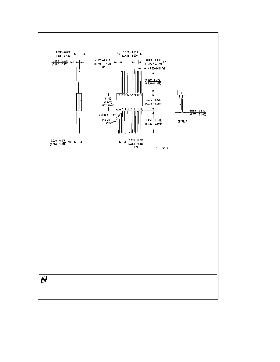
Physical Dimensions
inches (millimeters)
20-Lead Ceramic Leadless Chip Carrier (L)
NS Package Number E20A
5

Physical Dimensions
inches (millimeters) (Continued)
16-Lead Ceramic Dual-In-Line Package (D)
NS Package Number J16A
16-Lead (0 150 Wide) Molded Small Outline Package JEDEC (S)
NS Package Number M16A
6

Physical Dimensions
inches (millimeters) (Continued)
16-Lead (0 300 Wide) Molded Small Outline Package EIAJ (SJ)
NS Package Number M16D
16-Lead (0 300 Wide) Molded Dual-In-Line Package (P)
NS Package Number N16E
7
54F74F194
4-Bit
Bidirectional
Universal
Shift
Register
Physical Dimensions
inches (millimeters) (Continued)
16-Lead Ceramic Flatpak (F)
NS Package Number W16A
LIFE SUPPORT POLICY
NATIONAL'S PRODUCTS ARE NOT AUTHORIZED FOR USE AS CRITICAL COMPONENTS IN LIFE SUPPORT
DEVICES OR SYSTEMS WITHOUT THE EXPRESS WRITTEN APPROVAL OF THE PRESIDENT OF NATIONAL
SEMICONDUCTOR CORPORATION As used herein
1 Life support devices or systems are devices or
2 A critical component is any component of a life
systems which (a) are intended for surgical implant
support device or system whose failure to perform can
into the body or (b) support or sustain life and whose
be reasonably expected to cause the failure of the life
failure to perform when properly used in accordance
support device or system or to affect its safety or
with instructions for use provided in the labeling can
effectiveness
be reasonably expected to result in a significant injury
to the user
National Semiconductor
National Semiconductor
National Semiconductor
National Semiconductor
Corporation
Europe
Hong Kong Ltd
Japan Ltd
1111 West Bardin Road
Fax (a49) 0-180-530 85 86
13th Floor Straight Block
Tel 81-043-299-2309
Arlington TX 76017
Email cnjwge tevm2 nsc com
Ocean Centre 5 Canton Rd
Fax 81-043-299-2408
Tel 1(800) 272-9959
Deutsch Tel (a49) 0-180-530 85 85
Tsimshatsui Kowloon
Fax 1(800) 737-7018
English
Tel (a49) 0-180-532 78 32
Hong Kong
Fran ais Tel (a49) 0-180-532 93 58
Tel (852) 2737-1600
Italiano
Tel (a49) 0-180-534 16 80
Fax (852) 2736-9960
National does not assume any responsibility for use of any circuitry described no circuit patent licenses are implied and National reserves the right at any time without notice to change said circuitry and specifications