
TL F 12151
74F2245
Octal
Bidirectional
Transceiver
with
TRI-STATE
Outputs
November 1996
74F2245
Octal Bidirectional Transceiver with TRI-STATE
Outputs
General Description
The 'F2245 contains eight non-inverting bidirectional buffers
with TRI-STATE outputs and is intended for bus-oriented
applications Current sinking capability is 24 mA at the A
ports and 12 mA at the B ports The Transmit Receive
(T R) input determines the direction of data flow through
the bidirectional transceiver Transmit (active HIGH) en-
ables data from A ports to B ports Receive (active LOW)
enables data from B ports to A ports The Output Enable
input when HIGH disables both A and B ports by placing
them in a High Z condition
The 25X series resistors in the outputs reduce ringing and
eliminate the need for external resistors
Features
Y
Non-inverting buffers
Y
Bidirectional data path
Y
A outputs sink 24 mA
Y
B outputs sink 12 mA
Y
25X series resistors in B outputs eliminate the need for
external resistors
Y
Guaranteed 2000V minimum ESD protection
Commercial
Package
Package Description
Number
74F2245SC (Note 1)
M20B
20-Lead (0 300 Wide) Molded Small Outline JEDEC
Note 1
Devices also available in 13
reel Use suffix
e
SCX
Logic Symbols
TL F 12151 � 1
IEEE IEC
TL F 12151 � 2
TRI-STATE
is a registered trademark of National Semiconductor Corporation
C1996 National Semiconductor Corporation
RRD-B30M126 Printed in U S A
http
www national com

Connection Diagram
Pin Assignment for
DIP SOIC and SSOP
TL F 12151 � 3
Unit Loading Fan Out
74F
Pin Names
Description
U L
Input I
IH
I
IL
HIGH LOW
Output I
OH
I
OL
OE
Output Enable Input (Active LOW)
1 0 2 0
20 mA
b
1 2 mA
T R
Transmit Receive Input
1 0 2 0
20 mA
b
1 2 mA
A
0
� A
7
Side A Inputs or
3 5 1 083
70 mA
b
0 65 mA
TRI-STATE Outputs
150 40(38 3)
b
3 mA 24 mA
B
0
� B
7
Side B Inputs or
3 5 1 083
70 mA
b
0 65 mA
TRI-STATE Outputs
750 20
b
15 mA 12 mA
Truth Table
Inputs
Output
OE
T R
L
L
Bus B Data to Bus A
L
H
Bus A Data to Bus B
H
X
High Z State
H
e
HIGH Voltage Level
L
e
LOW Voltage Level
X
e
Immaterial
http
www national com
2

Absolute Maximum Ratings
(Note 1)
Storage Temperature
b
65 C to
a
150 C
Ambient Temperature under Bias
b
55 C to
a
125 C
Junction Temperature under Bias
Plastic
b
55 C to
a
150 C
V
CC
Pin Potential to
Ground Pin
b
0 5V to
a
7 0V
Input Voltage (Note 2)
b
0 5V to
a
7 0V
Input Current (Note 2)
b
30 mA to
a
5 0 mA
Voltage Applied to Output
in HIGH State (with V
CC
e
0V)
Standard Output
b
0 5V to V
CC
TRI-STATE Output
b
0 5V to
a
5 5V
Current Applied to Output
in LOW State (Max)
twice the rated I
OL
(mA)
ESD Last Passing Voltage (Min)
4000V
Note 1
Absolute maximum ratings are values beyond which the device may
be damaged or have its useful life impaired Functional operation under
these conditions is not implied
Note 2
Either voltage limit or current limit is sufficient to protect inputs
Recommended Operating
Conditions
Free Air Ambient Temperature
Commercial
0 C to
a
70 C
Supply Voltage
Commercial
a
4 5V to
a
5 5V
DC Electrical Characteristics
Symbol
Parameter
74F
Units
V
CC
Conditions
Min
Typ
Max
V
IH
Input HIGH Voltage
2 0
V
Recognized as a HIGH Signal
V
IL
Input LOW Voltage
0 8
V
Recognized as a LOW Signal
V
CD
Input Clamp Diode Voltage
b
1 2
V
Min
I
IN
e b
18 mA
V
OH
Output HIGH
10% V
CC
2 4
I
OH
e b
3 mA (A
n
)
Voltage
10% V
CC
2 0
V
Min
I
OH
e b
15 mA (B
n
)
5% V
CC
2 7
I
OH
e b
3 mA (A
n
)
V
OL
Output LOW
10% V
CC
0 5
I
OL
e
24 mA (A
n
)
Voltage
10% V
CC
0 5
V
Min
I
OL
e
1 mA (B
n
)
10% V
CC
0 75
I
OL
e
12 mA (B
n
)
I
IH
Input HIGH
5 0
m
A
Max
V
IN
e
2 7V
Current
I
BVI
Input HIGH Current
7 0
m
A
Max
V
IN
e
7 0V (OE T R)
Breakdown Test
I
BVIT
Input HIGH Current
0 5
mA
Max
V
IN
e
5 5 V (A
n
B
n
)
Breakdown (I O)
I
CEX
Output HIGH
50
m
A
Max
V
OUT
e
V
CC
(A
n
B
n
)
Leakage Current
V
ID
Input Leakage
4 75
V
0 0
I
ID
e
1 9 mA
Test
All Other Pins Grounded
I
OD
Output Leakage
3 75
m
A
0 0
V
IOD
e
150 mV
Circuit Current
All Other Pins Grounded
I
IL
Input LOW Current
b
1 2
mA
Max
V
IN
e
0 5V (T R OE)
I
IH
a
I
OZH
Output Leakage Current
70
m
A
Max
V
OUT
e
2 7V (A
n
B
n
)
I
IL
a
I
OZL
Output Leakage Current
b
650
m
A
Max
V
OUT
e
0 5V (A
n
B
n
)
http
www national com
3
DC Electrical Characteristics
(Continued)
Symbol
Parameter
74F
Units
V
CC
Conditions
Min
Typ
Max
I
OS
Output Short-Circuit Current
b
60
b
150
mA
Max
V
OUT
e
0V (A
n
)
b
100
b
225
V
OUT
e
0V (B
n
)
I
ZZ
Bus Drainage Test
500
m
A
0 0V
V
OUT
e
5 25V(A
n
B
n
)
I
CCH
Power Supply Current
70
90
mA
Max
V
O
e
HIGH
I
CCL
Power Supply Current
95
120
mA
Max
V
O
e
LOW
I
CCZ
Power Supply Current
85
110
mA
Max
V
O
e
HIGH Z
AC Electrical Characteristics
74F
74F
T
A
e a
25 C
T
A
V
CC
e
Com
Symbol
Parameter
V
CC
e a
5 0V
C
L
e
50 pF
Units
C
L
e
50 pF
Min
Typ
Max
Min
Max
t
PLH
Propagation Delay
2 5
4 2
6 5
2 0
7 5
ns
t
PHL
A
n
to B
n
or B
n
to A
n
2 5
4 2
7 5
2 0
8 5
t
PZH
Output Enable Time
3 0
5 3
8 0
2 5
9 0
t
PZL
3 5
6 0
10 0
3 0
11 0
ns
t
PHZ
Output Disable Time
2 0
5 0
6 5
2 0
7 5
t
PLZ
2 0
5 0
6 5
2 0
7 5
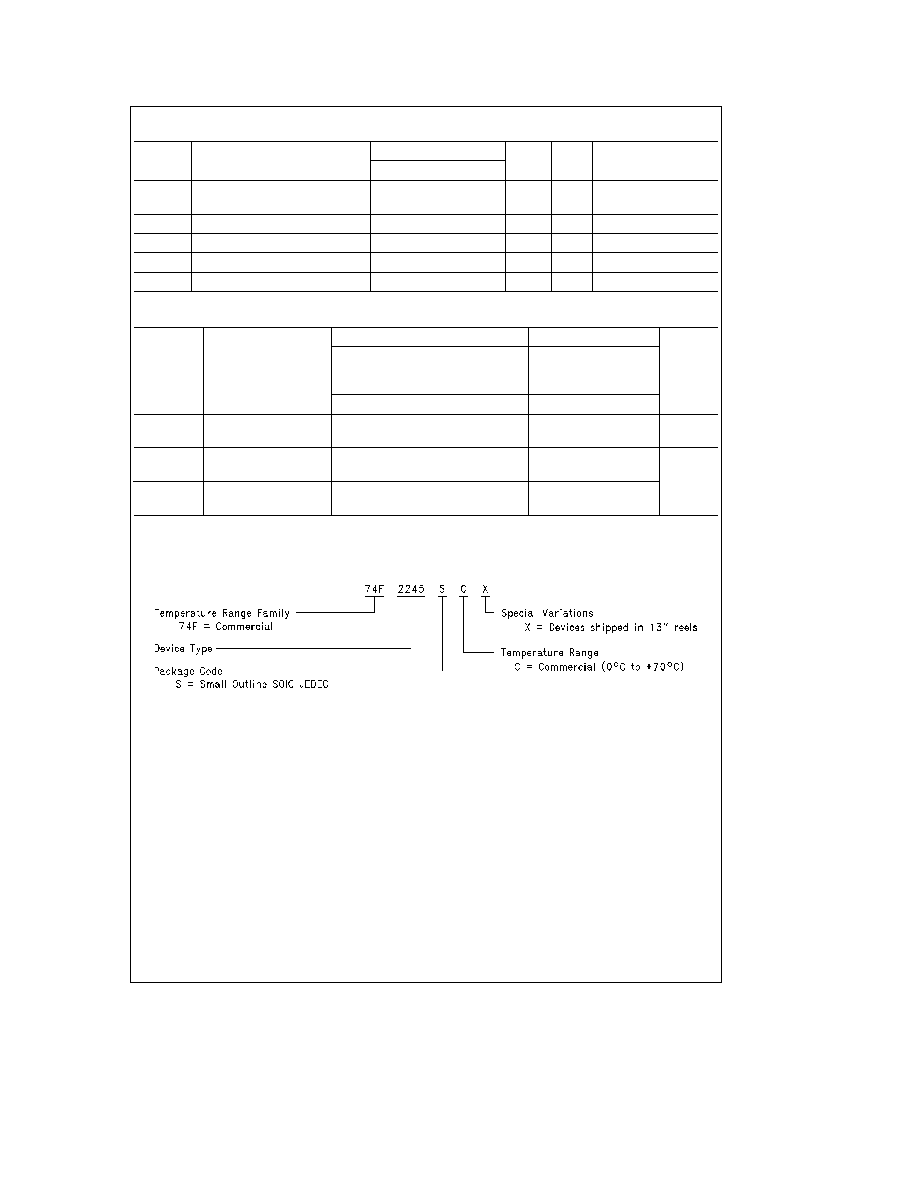
Ordering Information
The device number is used to form part of a simplified purchasing code where the package type and temperature range are
defined as follows
TL F 12151 � 4
http
www national com
4

http
www national com
5

74F2245
Octal
Bidirectional
Transceiver
with
TRI-STATE
Outputs
Physical Dimensions
inches (millimeters) unless otherwise noted
20-Lead (0 300 Wide) Molded Small Outline Package JEDEC (S)
NS Package Number M20B
LIFE SUPPORT POLICY
NATIONAL'S PRODUCTS ARE NOT AUTHORIZED FOR USE AS CRITICAL COMPONENTS IN LIFE SUPPORT
DEVICES OR SYSTEMS WITHOUT THE EXPRESS WRITTEN APPROVAL OF THE PRESIDENT OF NATIONAL
SEMICONDUCTOR CORPORATION As used herein
1 Life support devices or systems are devices or
2 A critical component is any component of a life
systems which (a) are intended for surgical implant
support device or system whose failure to perform can
into the body or (b) support or sustain life and whose
be reasonably expected to cause the failure of the life
failure to perform when properly used in accordance
support device or system or to affect its safety or
with instructions for use provided in the labeling can
effectiveness
be reasonably expected to result in a significant injury
to the user
National Semiconductor
National Semiconductor
National Semiconductor
National Semiconductor
Corporation
Europe
Southeast Asia
Japan Ltd
Fax a49 (0) 180-530 85 86
Fax (852) 2376 3901
Tel 81-3-5620-7561
Americas
Email europe support nsc com
Email sea support nsc com
Fax 81-3-5620-6179
Tel 1(800) 272-9959
Deutsch Tel a49 (0) 180-530 85 85
Fax 1(800) 737-7018
English
Tel a49 (0) 180-532 78 32
Email support nsc com
Fran ais Tel a49 (0) 180-532 93 58
Italiano
Tel a49 (0) 180-534 16 80
http
www national com
National does not assume any responsibility for use of any circuitry described no circuit patent licenses are implied and National reserves the right at any time without notice to change said circuitry and specifications