TL F 9541
54F74F413
6
4
x
4
First-In
First-Out
Buffer
Memory
with
Parallel
IO
January 1995
54F 74F413
64 x 4 First-In First-Out Buffer Memory with Parallel I O
General Description
The 'F413 is an expandable fall-through type high-speed
First-In First-Out (FIFO) buffer memory organized as 64
words by four bits The 4-bit input and output registers rec-
ord and transmit respectively asynchronous data in parallel
form Control pins on the input and output allow for hand-
shaking and expansion The 4-bit wide 62-bit deep fall-
through stack has self-contained control logic
Features
Y
Separate input and output clocks
Y
Parallel input and output
Y
Expandable without external logic
Y
15 MHz data rate
Y
Supply current 160 mA max
Y
Available in SOIC (300 mil only)
Commercial
Military
Package
Package Description
Number
74F413PC
N16E
16-Lead (0 300 Wide) Molded Dual-In-Line
54F413DM (Note 1)
J16A
16-Lead Ceramic Dual-In-Line
Note 1
Military grade device with environmental and burn-in processing Use suffix
e
DMQB
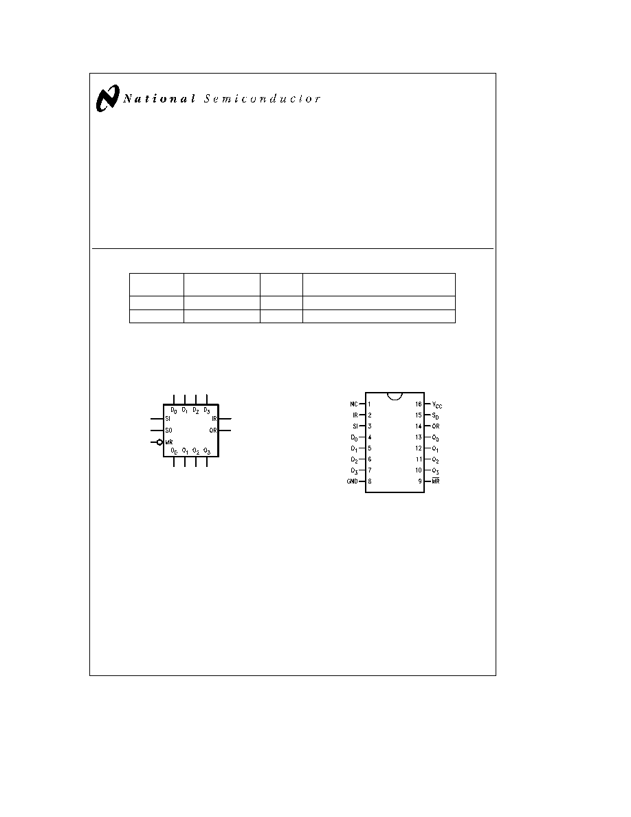
Logic Symbol
TL F 9541 � 1
Connection Diagram
Pin Assignment
for DIP
TL F 9541 � 2
TRI-STATE
is a registered trademark of National Semiconductor Corporation
C1995 National Semiconductor Corporation
RRD-B30M105 Printed in U S A

Unit Loading Fan Out
54F 74F
Pin Names
Description
U L
Input I
IH
I
IL
HIGH LOW
Output I
OH
I
OL
D
0
� D
3
Data Inputs
1 0 0 667
20 mA
b
0 4 mA
O
0
� O
3
Data Outputs
50 13 3
b
1 mA 8 mA
IR
Input Ready
1 0 0 667
20 mA
b
0 4 mA
SI
Shift In
1 0 0 667
20 mA
b
0 4 mA
SO
Shift Out
1 0 0 667
20 mA
b
0 4 mA
OR
Output Ready
1 0 0 667
20 mA
b
0 4 mA
MR
Master Reset
1 0 0 667
20 mA
b
0 4 mA
Functional Description
Data Input
Data is entered into the FIFO on D
0
� D
3
in-
puts To enter data the Input Ready (IR) should be HIGH
indicating that the first location is ready to accept data Data
then present at the four data inputs is entered into the first
location when the Shift In (SI) is brought HIGH An SI HIGH
signal causes the IR to go LOW Data remains at the first
location until SI is brought LOW When SI is brought LOW
and the FIFO is not full IR will go HIGH indicating that more
room is available Simultaneously data will propagate to the
second location and continue shifting until it reaches the
output stage or a full location If the memory is full IR will
remain LOW
Data Transfer
Once data is entered into the second cell
the transfer of any full cell to the adjacent (downstream)
empty cell is automatic activated by an on-chip control
Thus data will stack up at the end of the device while empty
locations will ``bubble'' to the front The t
PT
parameter de-
fines the time required for the first data to travel from input
to the output of a previously empty device
Data Output
Data is read from the O
0
� O
3
outputs When
data is shifted to the output stage Output Ready (OR) goes
HIGH indicating the presence of valid data When the OR is
HIGH data may be shifted out by bringing the Shift Out (SO)
HIGH A HIGH signal at SO causes the OR to go LOW Valid
data is maintained while the SO is HIGH When SO is
brought LOW the upstream data provided that stage has
valid data is shifted to the output stage When new valid
data is shifted to the output stage OR goes HIGH If the
FIFO is emptied OR stays LOW and O
0
� O
3
remains as
before i e data does not change if FIFO is empty
Input Ready and Output Ready
may also be used as
status signals indicating that the FIFO is completely full (In-
put Ready stays LOW for at least t
PT
) or completely empty
(Output Ready stays LOW for at least t
PT
)
Block Diagram
TL F 9541 � 4
2

Absolute Maximum Ratings
(Note 1)
If Military Aerospace specified devices are required
please contact the National Semiconductor Sales
Office Distributors for availability and specifications
Storage Temperature
b
65 C to
a
150 C
Ambient Temperature under Bias
b
55 C to
a
125 C
Junction Temperature under Bias
b
55 C to
a
175 C
Plastic
b
55 C to
a
150 C
V
CC
Pin Potential to
Ground Pin
b
0 5V to
a
7 0V
Input Voltage (Note 2)
b
0 5V to
a
7 0V
Input Current (Note 2)
b
30 mA to
a
5 0 mA
Voltage Applied to Output
in HIGH State (with V
CC
e
0V)
Standard Output
b
0 5V to V
CC
TRI-STATE Output
b
0 5V to
a
5 5V
Current Applied to Output
in LOW State (Max)
twice the rated I
OL
(mA)
Note 1
Absolute maximum ratings are values beyond which the device may
be damaged or have its useful life impaired Functional operation under
these conditions is not implied
Note 2
Either voltage limit or current limit is sufficient to protect inputs
Recommended Operating
Conditions
Free Air Ambient Temperature
Military
b
55 C to
a
125 C
Commercial
0 C to
a
70 C
Supply Voltage
Military
a
4 5V to
a
5 5V
Commercial
a
4 5V to
a
5 5V
DC Electrical Characteristics
Symbol
Parameter
54F 74F
Units
V
CC
Conditions
Min
Typ
Max
V
IH
Input HIGH Voltage
2 0
V
Recognized as a HIGH Signal
V
IL
Input LOW Voltage
0 8
V
Recognized as a LOW Signal
V
CD
Input Clamp Diode Voltage
b
1 5
V
Min
I
IN
e b
18 mA
V
OH
Output HIGH
54F 10% V
CC
2 4
I
OH
e b
1 mA
Voltage
74F 10% V
CC
2 4
V
Min
I
OH
e b
1 mA
74F 5% V
CC
2 7
I
OH
e b
1 mA
V
OL
Output LOW
54F 10% V
CC
0 5
V
Min
I
OL
e
8 mA
Voltage
74F 10% V
CC
0 5
I
OL
e
8 mA
I
IH
Input HIGH
54F
20 0
m
A
Max
V
IN
e
2 7V
Current
74F
5 0
I
BVI
Input HIGH Current 54F
100
m
A
Max
V
IN
e
7 0V
Breakdown Test
74F
7 0
I
CEX
Output HIGH
54F
250
m
A
Max
V
OUT
e
V
CC
Leakage Current
74F
50
V
ID
Input Leakage
74F
4 75
V
0 0
I
ID
e
1 9 mA
Test
All Other Pins Grounded
I
OD
Output Leakage
74F
3 75
m
A
0 0
V
IOD
e
150 mV
Circuit Current
All Other Pins Grounded
I
IL
Input LOW Current
b
0 4
mA
Max
V
IN
e
0 5V
I
OS
Output Short-Circuit Current
b
20
b
130
mA
Max
V
OUT
e
0V
I
CCH
Power Supply Current
115
160
mA
Max
V
O
e
HIGH
3

AC Electrical Characteristics
74F
54F
74F
T
A
e a
25 C
T
A
V
CC
e
Mil
T
A
V
CC
e
Com
Symbol
Parameter
V
CC
e a
5 0V
C
L
e
50 pF
C
L
e
50 pF
Units
C
L
e
50 pF
Min
Typ
Max
Min
Max
Min
Max
f
max
Shift In Rate
10
8 0
10
MHz
f
max
Shift Out Rate
10
8 0
10
MHz
t
PLH
Propagation Delay
1 5
44 0
1 5
50 0
1 5
48 0
ns
t
PHL
Shift In to IR
1 5
31 0
1 5
37 0
1 5
35 0
t
PLH
Propagation Delay
1 5
52 0
1 5
57 0
1 5
55 0
ns
t
PHL
Shift Out to OR
1 5
31 0
1 5
37 0
1 5
35 0
t
PLH
Propagation Delay
1 5
46 0
1 5
52 0
1 5
50 0
ns
t
PHL
Output Data Delay
1 5
34 0
1 5
39 0
1 5
37 0
t
PLH
Propagation Delay
1 5
27 0
1 5
33 0
1 5
31 0
ns
Master Reset to IR
t
PLH
Propagation Delay
1 5
30 0
1 5
34 0
1 5
32 0
ns
Master Reset to OR
AC Operating Requirements
74F
54F
74F
Symbol
Parameter
T
A
e a
25 C
T
A
V
CC
e
Mil
T
A
V
CC
e
Com
Units
V
CC
e a
5 0V
Min
Max
Min
Max
Min
Max
t
s
(H)
Setup Time HIGH or LOW
1 0
1 0
1 0
t
s
(L)
D
n
to SI
1 0
1 0
1 0
ns
t
h
(H)
Hold Time HIGH or LOW
10 0
10 0
10 0
t
h
(L)
D
n
to SI
10 0
10 0
10 0
t
w
(H)
Shift In Pulse Width
5 0
5 0
5 0
t
w
(L)
HIGH or LOW
10 0
10 0
10 0
ns
t
w
(H)
Shift Out Pulse Width
7 5
8 5
7 5
t
w
(L)
HIGH or LOW
10 0
10 0
10 0
t
w
(H)
Input Ready Pulse Width
7 5
8 5
7 5
ns
HIGH
t
w
(L)
Output Ready Pulse Width
5 0
5 0
5 0
ns
LOW
t
w
(L)
Master Reset Pulse Width
10 0
10 0
10 0
ns
LOW
t
rec
Recovery Time MR to SI
32 0
35 0
35 0
ns
t
PT
Data Throughput Time
0 9
1 0
1 0
m
s
4

Ordering Information
The device number is used to form part of a simplified purchasing code where the package type and temperature range are
defined as follows
74F
413
P
C
X
Temperature Range Family
Special Variations
74F
e
Commercial
QB
e
Military grade device with
54F
e
Military
environmental and burn-in
processing
Device Type
Temperature Range
Package Code
C
e
Commercial (0 C to
a
70 C)
P
e
Plastic DIP
M
e
Military (
b
55 C to
a
125 C)
D
e
Ceramic DIP
Physical Dimensions
inches (millimeters)
16-Lead Ceramic Dual-In-Line Package (D)
NS Package Number J16A
5

54F74F413
6
4
x
4
First-In
First-Out
Buffer
Memory
with
Parallel
IO
Physical Dimensions
inches (millimeters) (Continued)
16-Lead (0 300 Wide) Molded Dual-In-Line Package (P)
NS Package Number N16E
LIFE SUPPORT POLICY
NATIONAL'S PRODUCTS ARE NOT AUTHORIZED FOR USE AS CRITICAL COMPONENTS IN LIFE SUPPORT
DEVICES OR SYSTEMS WITHOUT THE EXPRESS WRITTEN APPROVAL OF THE PRESIDENT OF NATIONAL
SEMICONDUCTOR CORPORATION As used herein
1 Life support devices or systems are devices or
2 A critical component is any component of a life
systems which (a) are intended for surgical implant
support device or system whose failure to perform can
into the body or (b) support or sustain life and whose
be reasonably expected to cause the failure of the life
failure to perform when properly used in accordance
support device or system or to affect its safety or
with instructions for use provided in the labeling can
effectiveness
be reasonably expected to result in a significant injury
to the user
National Semiconductor
National Semiconductor
National Semiconductor
National Semiconductor
Corporation
Europe
Hong Kong Ltd
Japan Ltd
1111 West Bardin Road
Fax (a49) 0-180-530 85 86
13th Floor Straight Block
Tel 81-043-299-2309
Arlington TX 76017
Email cnjwge tevm2 nsc com
Ocean Centre 5 Canton Rd
Fax 81-043-299-2408
Tel 1(800) 272-9959
Deutsch Tel (a49) 0-180-530 85 85
Tsimshatsui Kowloon
Fax 1(800) 737-7018
English
Tel (a49) 0-180-532 78 32
Hong Kong
Fran ais Tel (a49) 0-180-532 93 58
Tel (852) 2737-1600
Italiano
Tel (a49) 0-180-534 16 80
Fax (852) 2736-9960
National does not assume any responsibility for use of any circuitry described no circuit patent licenses are implied and National reserves the right at any time without notice to change said circuitry and specifications