TL F 9580
54F74F646
74F646B
54F74F648
Octal
TransceiverRegister
with
TRI-STATE
Outputs
December 1994
54F 74F646
74F646B
54F 74F648
Octal Transceiver Register with TRI-STATE
Outputs
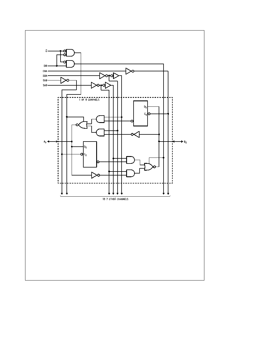
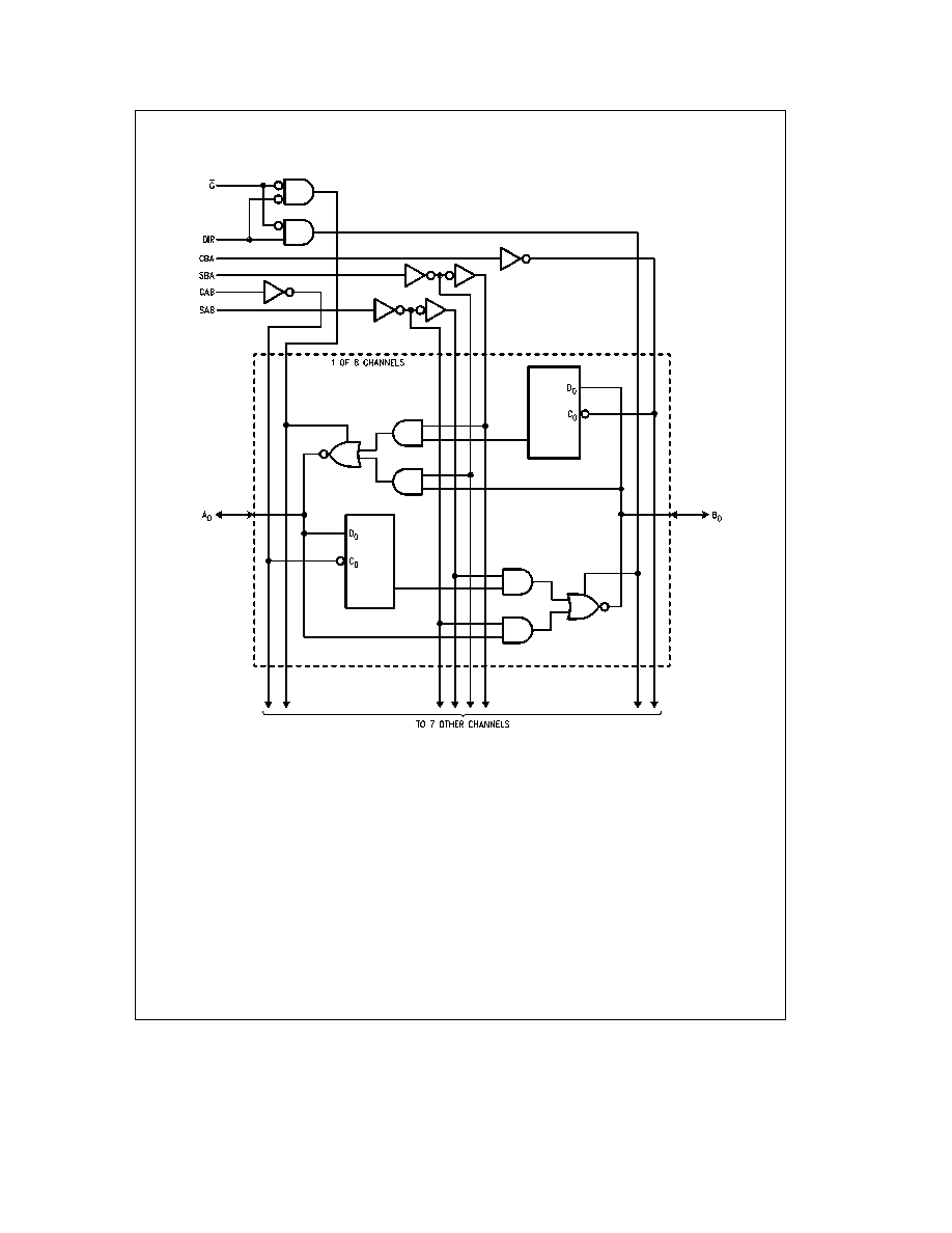
General Description
These devices consist of bus transceiver circuits with TRI-
STATE D-type flip-flops and control circuitry arranged for
multiplexed transmission of data directly from the input bus
or from the internal registers Data on the A or B bus will be
clocked into the registers as the appropriate clock pin goes
to a high logic level Control G and direction pins are provid-
ed to control the transceiver function In the transceiver
mode data present at the high impedance port may be
stored in either the A or the B register or in both The select
controls can multiplex stored and real-time (transparent
mode) data The direction control determines which bus will
receive data when the enable control G is Active LOW In
the isolation mode (control G HIGH) A data may be stored
in the B register and or B data may be stored in the A regis-
ter
Features
Y
Independent registers for A and B buses
Y
Multiplexed real-time and stored data
Y
'F648 has inverting data paths
Y
'F646 'F646B have non-inverting data paths
Y
'F646B is a faster version of the 'F646
Y
TRI-STATE outputs
Y
300 mil slim DIP
Y
Guaranteed 4000V minimum ESD protection
Commercial
Military
Package
Package Description
Number
74F646SPC
N24C
24-Lead (0 300 Wide) Molded Dual-In-Line
54F646DM (Note 2)
J24F
24-Lead (0 300 Wide) Ceramic Dual-In-Line
74F646SC (Note 1)
M24B
24-Lead (0 300 Wide) Molded Small Outline JEDEC
74F646MSA (Note 1)
MSA24
24-Lead Molded Shrink Small Outline EIAJ Type II
54F646FM (Note 2)
W24C
24-Lead Cerpack
54F646LM (Note 2)
E28A
28-Lead Ceramic Leadless Chip Carrier Type C
74F646BSPC
N24C
24-Lead (0 300 Wide) Molded Dual-In-Line
74F646BSC (Note 1)
M24B
24-Lead (0 300 Wide) Molded Small Outline JEDEC
74F648SPC
N24C
24-Lead (0 300 Wide) Molded Dual-In-Line
54F648SDM (Note 2)
J24F
24-Lead (0 300 Wide) Ceramic Dual-In-Line
74F648SC (Note 1)
M24B
24-Lead (0 300 Wide) Molded Small Outline JEDEC
54F648FM (Note 2)
W24C
24-Lead Cerpack
54F648LM (Note 2)
E28A
24-Lead Ceramic Leadless Chip Carrier Type C
Note 1
Devices also available in 13
reel Use suffix
e
SCX
Note 2
Military grade device with environmental and burn-in processing Use suffix
e
DMQB FMQB and LMQB
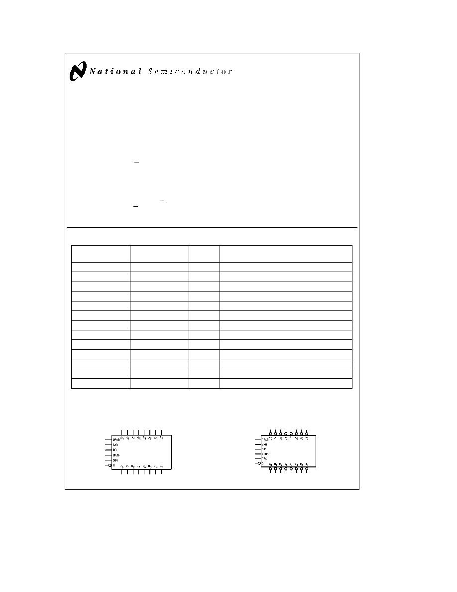
Logic Symbols
'F646 'F646B
TL F 9580 ≠ 1
'F648
TL F 9580 ≠ 7
TRI-STATE
is a registered trademark of National Semiconductor Corporation
C1995 National Semiconductor Corporation
RRD-B30M75 Printed in U S A
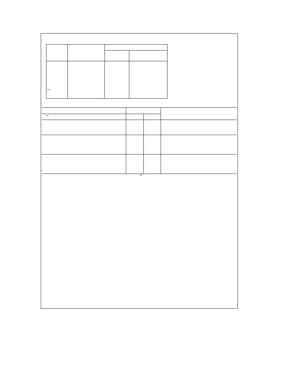
Unit Loading Fan Out
54F 74F
Pin Names
Description
U L
Input I
IH
I
IL
HIGH LOW
Output I
OH
I
OL
A
0
≠ A
7
Data Register A Inputs
3 5 1 083
70 mA
b
650 mA
TRI-STATE Outputs
600 106 6 (80)
b
12 mA 64 mA (48 mA)
B
0
≠ B
7
Data Register B Inputs
3 5 1 083
70 mA
b
650 mA
TRI-STATE Outputs
600 106 6 (80)
b
12 mA 64 mA (48 mA)
CPAB CPBA Clock Pulse Inputs
1 0 1 0
20 mA
b
0 6 mA
SAB SBA
Select Inputs
1 0 1 0
20 mA
b
0 6 mA
G
Output Enable Input
1 0 1 0
20 mA
b
0 6 mA
DIR
Direction Control Input
1 0 1 0
20 mA
b
0 6 mA
Function Table
Inputs
Data I O
Function
G
DIR
CPAB
CPBA
SAB
SBA
A
0
≠ A
7
B
0
≠ B
7
H
X
H or L
H or L
X
X
Isolation
H
X
L
X
X
X
Input
Input
Clock A
n
Data into A Register
H
X
X
L
X
X
Clock B
n
Data into B Register
L
H
X
X
L
X
A
n
to B
n
Real Time (Transparent Mode)
L
H
L
X
L
X
Input
Output
Clock A
n
Data into A Register
L
H
H or L
X
H
X
A Register to B
n
(Stored Mode)
L
H
L
X
H
X
Clock A
n
Data into A Register and Output to B
n
L
L
X
X
X
L
B
n
to A
n
Real Time (Transparent Mode)
L
L
X
L
X
L
Output
Input
Clock B
n
Data into B Register
L
L
X
H or L
X
H
B Register to A
n
(Stored Mode)
L
L
X
L
X
H
Clock B
n
Data into B Register and Output to A
n
The data output functions may be enabled or disabled by various signals at the G and DIR Inputs Data input functions are always enabled i e data at the bus
pins will be stored on every LOW-to-HIGH transition of the clock inputs
H
e
HIGH Voltage Level
L
e
LOW Voltage Level
X
e
Irrelevant
L
e
LOW-to-HIGH Transition
3