
TL F 10146
54FCT74FCT273
Octal
D
Flip-Flop
March 1993
54FCT 74FCT273
Octal D Flip-Flop
General Description
The 'FCT273 has eight edge-triggered D-type flip-flops with
individual D inputs and Q outputs The common buffered
Clock (CP) and Master Reset (MR) input load and reset
(clear) all flip-flops simultaneously
The register is fully edge-triggered The state of each D in-
put one setup time before the LOW-to-HIGH clock tran-
sition is transferred to the corresponding flip-flop's Q out-
put
All outputs will be forced LOW independently of Clock or
Data inputs by a LOW voltage level on the MR input The
device is useful for applications where the true output only is
required and the Clock and Master Reset are common to all
storage elements
Features
Y
I
CC
reduced to 40 0 mA
Y
Ideal buffer for MOS microprocessor or memory
Y
Eight edge-triggered D flip-flops
Y
Buffered common clock
Y
Buffered asynchronous master reset
Y
TTL input and output level compatible
Y
TTL levels accept CMOS levels
Y
I
OL
e
48 mA (Com) 32 mA (Mil)
Y
NSC 54 74FCT273 is pin and functionally equivalent to
IDT 54 74FCT273
Y
Military
product
compliant
to
MIL-STD-883
and
Standard Military Drawing
5962-87656
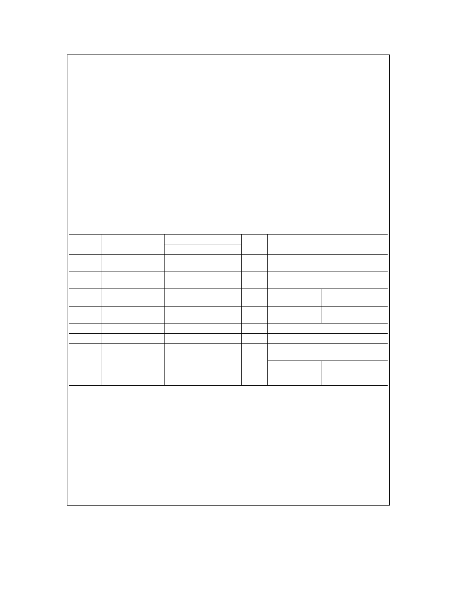
Logic Symbols
Connection Diagrams
TL F 10146 � 1
IEEE IEC
TL F 10146 � 2
Pin Assignment
for DIP Flatpak and SOIC
TL F 10146 � 3
Pin Names
Description
D
0
� D
7
Data Inputs
MR
Master Reset
CP
Clock Pulse Input
Q
0
� Q
7
Data Outputs
Pin Assignment
for LCC
TL F 10146 � 4
FACT
TM
is a trademark of National Semiconductor Corporation
C1995 National Semiconductor Corporation
RRD-B30M105 Printed in U S A

Mode Select-Function Table
Operating Mode
Inputs
Outputs
MR
CP
D
n
Q
n
Reset (Clear)
L
X
X
L
Load `1'
H
L
H
H
Load `0'
H
L
L
L
H
e
HIGH Voltage Level
L
e
LOW Voltage Level
X
e
Immaterial
L
e
LOW-to-HIGH Transition
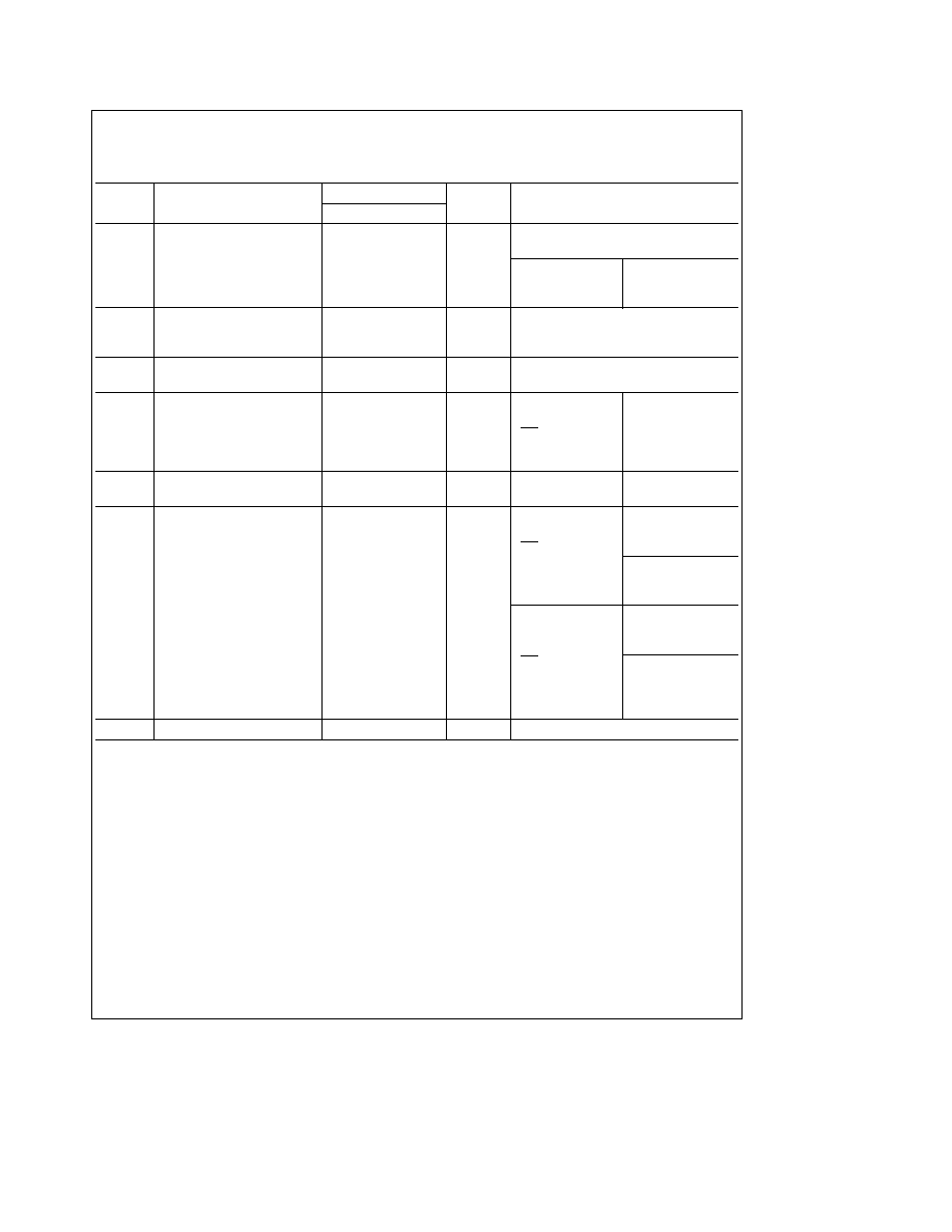
Logic Diagram
TL F 10146 � 5
Please note that this diagram is provided only for the understanding of logic operations and should not be used to estimate propagation delays
2
Absolute Maximum Ratings
(Note 1)
If Military Aerospace specified devices are required
please contact the National Semiconductor Sales
Office Distributors for availability and specifications
Terminal Voltage with Respect to GND
(V
TERM
)
54FCT
b
0 5 to
a
7 0V
74FCT
b
0 5 to
a
7 0V
Temperature Under Bias (T
BIAS
)
74FCT
b
55 C to
a
125 C
54FCT
b
65 C to
a
135 C
Storage Temperature (T
STG
)
74FCT
b
55 C to
a
125 C
54FCT
b
65 C to
a
150 C
DC Output Current (I
OUT
)
120 mA
Note 1
Absolute maximum ratings are those values beyond which damage
to the device may occur The databook specifications should be met without
exception to ensure that the system design is reliable over its power supply
temperature and output input loading variables National does not recom-
mend operation of FACT
TM
FCT circuits outside databook specifications
Recommended Operating
Conditions
Supply Voltage (V
CC
)
54FCT
4 5V to 5 5V
74FCT
4 75 to 5 25V
Input Voltage
0V to V
CC
Output Voltage
0V to V
CC
Operating Temperature (T
A
)
54FCT
b
55 C to
a
125 C
74FCT
0 C to
a
70 C
Junction Temperature (T
J
)
CDIP
175 C
PDIP
140 C
Note
All commercial packaging is not recommended for applications requir-
ing greater than 2000 temperature cycles from
b
40 C to
a
125 C
DC Characteristics for 'FCT Family Devices
Typical values are at V
CC
e
5 0V 25 C ambient and maximum loading For test conditions shown as Max use the value
specified for the appropriate device type Com V
CC
e
5 0V
g
5% T
A
e
0 C to
a
70 C Mil V
CC
e
5 0V
g
10% T
A
e b
55 C
to
a
125 C V
HC
e
V
CC
b
0 2V
Symbol
Parameter
54FCT 74FCT
Units
Conditions
Min
Typ
Max
V
IH
Minimum High Level
2 0
V
Input Voltage
V
IL
Maximum Low Level
0 8
V
Input Voltage
I
IH
Input High Current
5 0
m
A
V
CC
e
Max
V
I
e
V
CC
5 0
V
I
e
2 7V (Note 2)
I
IL
Input Low Current
b
5 0
m
A
V
CC
e
Max
V
I
e
0 5V (Note 2)
b
5 0
V
I
e
GND
V
IK
Clamp Diode Voltage
b
0 7
b
1 2
V
V
CC
e
Min I
N
e b
18 mA
I
OS
Short Circuit Current
b
60
b
120
mA
V
CC
e
Max (Note 1) V
O
e
GND
V
OH
Minimum High Level
2 8
3 0
V
CC
e
3V V
IN
e
0 2V or V
HC
Output Voltage
I
OL
e b
32 mA
V
HC
V
CC
V
V
CC
e
Min
I
OH
e b
300 mA
2 4
4 3
V
IN
e
V
IH
or V
IL
I
OH
e b
12 mA (Mil)
2 4
4 3
I
OH
e b
15 mA (Com)
3
DC Characteristics for 'FCT Family Devices
(Continued)
Typical values are at V
CC
e
5 0V 25 C ambient and maximum loading For test conditions shown as Max use the value
specified for the appropriate device type Com V
CC
e
5 0V
g
5% T
A
e
0 C to
a
70 C Mil V
CC
e
5 0V
g
10% T
A
e b
55 C
to
a
125 C V
HC
e
V
CC
b
0 2V
Symbol
Parameter
54FCT 74FCT
Units
Conditions
Min
Typ
Max
V
OL
Maximum Low Level
GND
0 2
V
V
CC
e
3V V
IN
e
0 2V or V
HC
Output Voltage
I
OL
e
300 mA
GND
0 2
V
CC
e
Min
I
OL
e
300 mA
0 3
0 5
V
IN
e
V
IH
or V
IL
I
OL
e
48 mA (Mil)
0 3
0 5
I
OL
e
32 mA (Com)
I
CC
Maximum Quiescent
V
CC
e
Max
Supply Current
1 0
40 0
m
A
V
IN
t
V
HC
V
IN
s
0 2V
f
I
e
0
D
I
CC
Quiescent Supply Current
0 5
2 0
mA
V
CC
e
Max
TTL Inputs HIGH
V
IN
e
3 4V (Note 3)
I
CCD
Dynamic Power
V
CC
Max
V
IN
t
V
HC
Supply Current (Note 4)
Outputs Open
V
IN
s
0 2V
0 25
0 40
mA MHz
MR
e
V
CC
One Input Toggling
50% Duty Cycle
V
H
Input Hysteresis
200
mV
on Clock Only
I
C
Total Power
V
CC
e
Max
V
IN
t
V
HC
Supply Current (Note 6)
1 5
4 0
Outputs Open
V
IN
s
0 2V
MR
e
V
CC
f
I
e
10 MHz
V
IN
e
3 4V
1 8
6 0
One Bit Toggling
V
IN
e
GND
50% Duty Cycle
mA
(Note 5)
V
IN
t
V
HC
3 0
7 8
V
CC
e
Max
V
IN
s
0 2V
Outputs Open
MR
e
V
CC
f
I
e
2 5 MHz
V
IN
e
3 4V
5 0
16 8
Eight Bits Toggling
V
IN
e
GND
50% Duty Cycle
V
H
Input Hysteresis on Clock Only
200
mV
Note 1
Maximum test duration not to exceed one second not more than one output shorted at one time
Note 2
This parameter guaranteed but not tested
Note 3
Per TTL driven input (V
IN
e
3 4V) all other inputs at V
CC
or GND
Note 4
This parameter is not directly testable but is derived for use in Total Power Supply calculations
Note 5
Values for these conditions are examples of the I
CC
formula These limits are guaranteed but not tested
Note 6
I
C
e
I
QUIESCENT
a
I
INPUTS
a
I
DYNAMIC
I
C
e
I
CC
a
D
I
CC
D
H
N
T
a
I
CCD
(f
CP
2
a
f
I
N
I
)
I
CC
e
Quiescent Current
D
I
CC
e
Power Supply Curent for a TTL High Input (V
IN
e
3 4V)
D
H
e
Duty Cycle for TTL inputs High
N
T
e
Number of Inputs at D
H
I
CCD
e
Dynamic Current Caused by an Input Transition Pair (HLH or LHL)
f
CP
e
Clock Frequency for Register Devices (Zero for Non-Register Devices)
f
I
e
Input Frequency
N
I
e
Number of Inputs at f
I
All currents are in milliamps and all frequencies are in megahertz
4

AC Electrical Characteristics
54FCT 74FCT
74FCT
54FCT
T
A
e a
25 C
T
A
V
CC
e
Com
T
A
V
CC
e
Mil
Symbol
Parameter
V
CC
e
5 0V
R
L
e
500X
R
L
e
500X
Units
C
L
e
50 pF
C
L
e
50 pF
Typ
Min
Max
Min
Max
t
PHL
Propagation Delay
7 0
2 0
13 0
1 5
9 5
ns
t
PLH
Clock to Output
t
PLH
Propagation Delay
8 0
2 0
13 0
1 5
10 5
ns
t
PHL
MR to Output
t
SU
Setup Time HIGH
1 5
3 0
3 5
ns
or LOW Data to CP
t
h
Hold Time HIGH
1 0
2 0
2 0
ns
or LOW Data to CP
t
w
Clock Pulse Width
4 0
7 0
5 0
ns
HIGH or LOW
t
w
MR Pulse Width
4 0
7 0
5 0
ns
HIGH or LOW
t
rec
Recovery Time
3 0
4 0
4 0
ns
MR to CP
f
max
Maximum Clock Frequency
90
MHz
Note 1
Minimum limits are guaranteed but not tested on Propagation Delays
Capacitance
T
A
e
25 C f
e
1 0 MHz
Symbol
Parameter
Conditions
Typ
Max
Unit
C
IN
Input Capacitance
V
IN
e
0V
6
10
pF
C
OUT
Output Capacitance
V
OUT
e
0V
8
12
pF
Note
This parameter is guaranteed by characterization data and not tested
Ordering Information
The device number is used to form part of a simplified purchasing code where the package type and temperature range are
defined as follows
74FCT
273
P
C
QR
Temperature Range Family
Special Variations
74FCT
e
Commercial TTL-Compatible
X
e
Devices shipped in 13 reels
54FCT
e
Military TTL-Compatible
QR
e
Commercial grade device with
burn-in
Device Type
QB
e
Military grade with
environmental and burn-in
Package Code
processing shipped in tubes
P
e
Plastic DIP
D
e
Ceramic DIP
Temperature Range
F
e
Flatpak
C
e
Commercial (0 C to
a
70 C)
L
e
Leadless Ceramic Chip Carrier (LCC)
M
e
Military (
b
55 C to
a
125 C)
S
e
Small Outline (SOIC)
5