TL F 11993
74LCX240
Low-Voltage
Octal
BufferLine
Driver
with
5V
Tolerant
Inputs
and
Outputs
December 1996
74LCX240
Low-Voltage Octal Buffer Line Driver
with 5V Tolerant Inputs and Outputs
General Description
The LCX240 is an inverting octal buffer and line driver de-
signed to be employed as a memory address driver clock
driver and bus oriented transmitter or receiver The device is
designed for low voltage (3 3V) V
CC
applications with capa-
bility of interfacing to a 5V signal environment
The LCX240 is fabricated with an advanced CMOS technol-
ogy to achieve high speed operation while maintaining
CMOS low power dissipation
Features
Y
5V tolerant inputs and outputs
Y
6 5 ns t
PD
max 10 mA I
CCQ
max
Y
Power-down high impedance inputs and outputs
Y
Supports live insertion withdrawal
Y
2 0V ≠ 3 6V V
CC
supply operation
Y
g
24 mA output drive
Y
Implements patented Quiet Series
TM
noise EMI
reduction circuitry
Y
Functionally compatible with the 74 series 240
Y
Latch-up performance exceeds 500 mA
Y
ESD performance
Human Body Model
l
2000V
Machine Model
l
200V
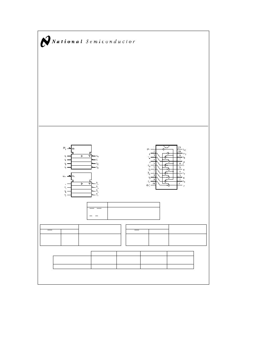
Logic Symbol
IEEE IEC
TL F 11993 ≠ 1
Connection Diagram
Pin Assignment
for SOIC SSOP and TSSOP
TL F 11993 ≠ 2
Pin Names
Description
OE
1
OE
2
TRI-STATE Output Enable Inputs
I
0
≠ I
7
Inputs
O
0
≠ O
7
Outputs
Truth Tables
Inputs
(Pins 12 14 16 18)
Outputs
OE
1
I
n
L
L
H
L
H
L
H
X
Z
Inputs
Outputs
OE
2
I
n
(Pins 3 5 7 9)
L
L
H
L
H
L
H
X
Z
H
e
HIGH Voltage Level
L
e
LOW Voltage Level
X
e
Immaterial
Z
e
High Impedance
SOIC JEDEC
SOIC EIAJ
SSOP Type II
TSSOP
Order Number
74LCX240WM
74LCX240SJ
74LCX240MSA
74LCX240MTC
74LCX240WMX
74LCX240SJX
74LCX240MSAX
74LCX240MTCX
See NS Package Number
M20B
M20D
MSA20
MTC20
TRI-STATE
is a registered trademark of National Semiconductor Corporation
Quiet Series
TM
is a trademark of National Semiconductor Corporation
C1996 National Semiconductor Corporation
RRD-B30M17 Printed in U S A
http
www national com

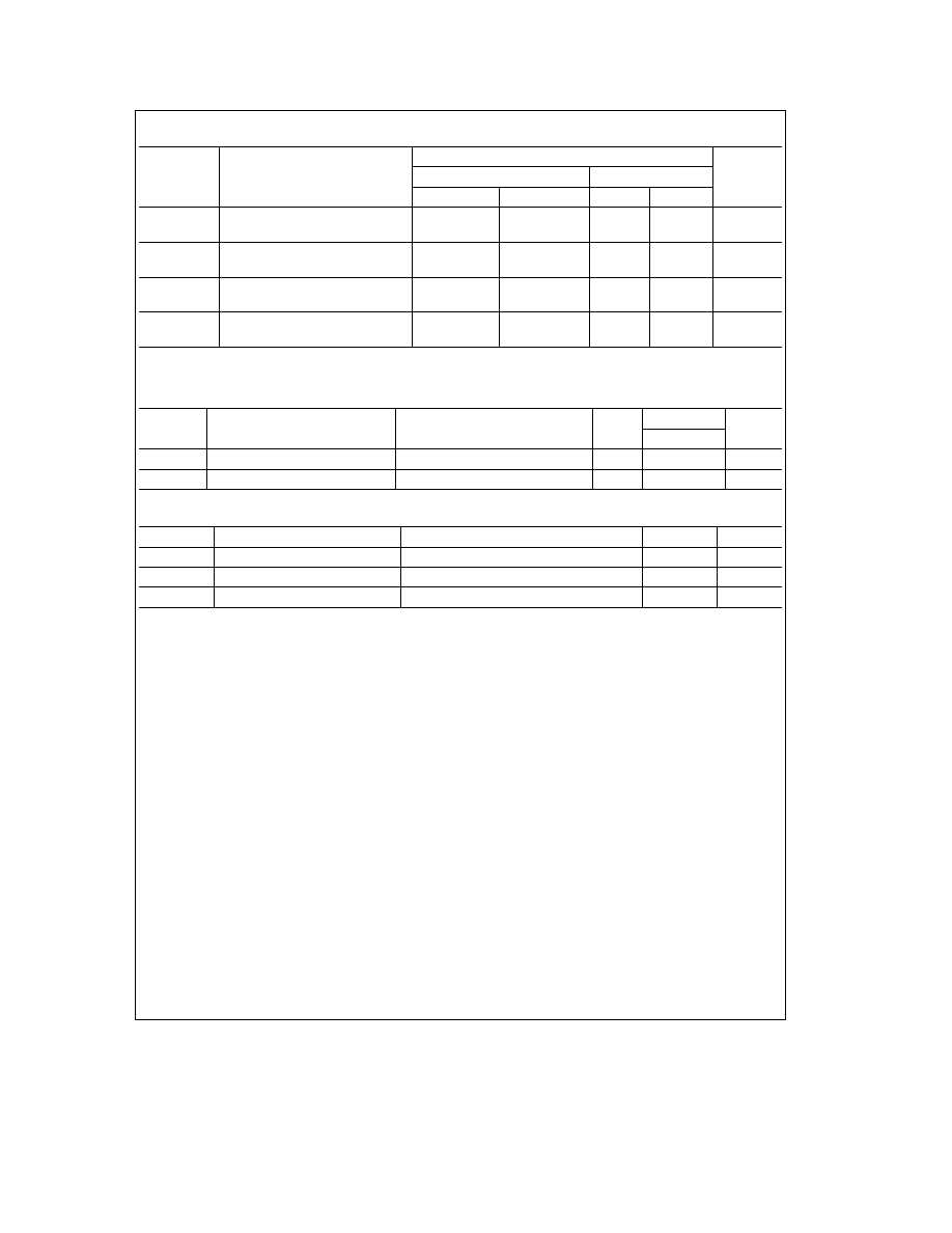
Absolute Maximum Ratings
(Note 1)
If Military Aerospace specified devices are required please contact the National Semiconductor Sales Office
Distributors for availability and specifications
Symbol
Parameter
Value
Conditions
Units
V
CC
Supply Voltage
b
0 5 to
a
7 0
V
V
I
DC Input Voltage
b
0 5 to
a
7 0
V
V
O
DC Output Voltage
b
0 5 to
a
7 0
Output in TRI-STATE
V
b
0 5 to V
CC
a
0 5
Output in High or Low State (Note 2)
V
I
IK
DC Input Diode Current
b
50
V
I
k
GND
mA
I
OK
DC Output Diode Current
b
50
V
O
k
GND
mA
a
50
V
O
l
V
CC
I
O
DC Output Source Sink Current
g
50
mA
I
CC
DC Supply Current per Supply Pin
g
100
mA
I
GND
DC Ground Current per Ground Pin
g
100
mA
T
STG
Storage Temperature
b
65 to
a
150
C
Note 1
The Absolute Maximum Ratings are those values beyond which the safety of the device cannot be guaranteed The device should not be operated at these
limits The parametric values defined in the ``Electrical Characteristics'' table are not guaranteed at the Absolute Maximum Ratings The ``Recommended Operating
Conditions'' table will define the conditions for actual device operation
Note 2
I
O
Absolute Maximum Rating must be observed
Recommended Operating Conditions
Symbol
Parameter
Min
Max
Units
V
CC
Supply Voltage
Operating
2 0
3 6
V
Data Retention
1 5
3 6
V
I
Input Voltage
0
5 5
V
V
O
Output Voltage
HIGH or LOW State
0
V
CC
V
TRI-STATE
0
5 5
I
OH
I
OL
Output Current
V
CC
e
3 0V ≠ 3 6V
g
24
mA
V
CC
e
2 7V
g
12
T
A
Free-Air Operating Temperature
b
40
85
C
D
t DV
Input Edge Rate V
IN
e
0 8V ≠ 2 0V V
CC
e
3 0V
0
10
ns V
DC Electrical Characteristics
Symbol
Parameter
Conditions
V
CC
T
A
e b
40 C to
a
85 C
Units
(V)
Min
Max
V
IH
HIGH Level Input Voltage
2 7 ≠ 3 6
2 0
V
V
IL
LOW Level Input Voltage
2 7 ≠ 3 6
0 8
V
V
OH
HIGH Level Output Voltage
I
OH
e b
100 mA
2 7 ≠ 3 6
V
CC
b
0 2
V
I
OH
e b
12 mA
2 7
2 2
V
I
OH
e b
18 mA
3 0
2 4
V
I
OH
e b
24 mA
3 0
2 2
V
V
OL
LOW Level Output Voltage
I
OL
e
100 mA
2 7 ≠ 3 6
0 2
V
I
OL
e
12 mA
2 7
0 4
V
I
OL
e
16 mA
3 0
0 4
V
I
OL
e
24 mA
3 0
0 55
V
I
I
Input Leakage Current
0
s
V
I
s
5 5V
2 7 ≠ 3 6
g
5 0
m
A
I
OZ
TRI-STATE Output Leakage
0
s
V
O
s
5 5V
2 7 ≠ 3 6
g
5 0
m
A
V
I
e
V
IH
or V
IL
I
OFF
Power-Off Leakage Current
V
I
or V
O
e
5 5V
0
10
m
A
I
CC
Quiescent Supply Current
V
I
e
V
CC
or GND
2 7 ≠ 3 6
10
m
A
3 6V
s
V
I
V
O
s
5 5V
2 7 ≠ 3 6
g
10
m
A
D
I
CC
Increase in I
CC
per Input
V
IH
e
V
CC
b
0 6V
2 7 ≠ 3 6
500
m
A
http
www national com
2
AC Electrical Characteristics
Symbol
Parameter
T
A
e b
40 C to
a
85 C
Units
V
CC
e
3 3V
g
0 3V
V
CC
e
2 7V
Min
Max
Min
Max
t
PHL
Propagation Delay
1 5
6 5
1 5
7 5
ns
t
PLH
Data to Output
1 5
6 5
1 5
7 5
t
PZL
Output Enable Time
1 5
8 0
1 5
9 0
ns
t
PZH
1 5
8 0
1 5
9 0
t
PLZ
Output Disable Time
1 5
7 0
1 5
8 0
ns
t
PHZ
1 5
7 0
1 5
8 0
t
OSHL
Output to Output Skew (Note 1)
1 0
ns
t
OSLH
1 0
Note 1
Skew is defined as the absolute value of the difference between the actual propagation delay for any two separate outputs of the same device The
specification applies to any outputs switching in the same direction either HIGH to LOW (t
OSHL
) or LOW to HIGH (t
OSLH
)
Dynamic Switching Characteristics
Symbol
Parameter
Conditions
V
CC
(V)
T
A
e
25 C
Units
Typical
V
OLP
Quiet Output Dynamic Peak V
OL
C
L
e
50 pF V
IH
e
3 3V V
IL
e
0V
3 3
0 8
V
V
OLV
Quiet Output Dynamic Valley V
OL
C
L
e
50 pF V
IH
e
3 3V V
IL
e
0V
3 3
b
0 8
V
Capacitance
Symbol
Parameter
Conditions
Typical
Units
C
IN
Input Capacitance
V
CC
e
Open V
I
e
0V or V
CC
7
pF
C
OUT
Output Capacitance
V
CC
e
3 3V V
I
e
0V or V
CC
8
pF
C
PD
Power Dissipation Capacitance
V
CC
e
3 3V V
I
e
0V or V
CC
F
e
10 MHz
25
pF
http
www national com
3

74LCX240 Ordering Information
The device number is used to form part of a simplified purchasing code where the package type and temperature range are
defined as follows
TL F 11993 ≠ 3
Physical Dimensions
inches (millimeters) unless otherwise noted
20-Lead Small Outline Integrated Circuit
Order Number 74LCX240WM or 74LCX240WMX
NS Package Number M20B
http
www national com
4

Physical Dimensions
inches (millimeters) unless otherwise noted (Continued)
20-Lead Small Outline Package EIAJ (SJ)
Order Number 74LCX240SJ or 74LCX240SJX
NS Package Number M20D
All dimensions are in millimeters
20-Lead Molded Shrink Small Outline Package EIAJ Type II
Order Number 74LCX240MSA or 74LCX240MSAX
NS Package Number MSA20
http
www national com
5