TL F 6381
DM74LS90DM74LS93
Decade
and
Binary
Counters
June 1989
DM74LS90 DM74LS93
Decade and Binary Counters
General Description
Each of these monolithic counters contains four master-
slave flip-flops and additional gating to provide a divide-by-
two counter and a three-stage binary counter for which the
count cycle length is divide-by-five for the 'LS90 and divide-
by-eight for the 'LS93
All of these counters have a gated zero reset and the LS90
also has gated set-to-nine inputs for use in BCD nine's com-
plement applications
To use their maximum count length (decade or four bit bina-
ry) the B input is connected to the Q
A
output The input
count pulses are applied to input A and the outputs are as
described in the appropriate truth table A symmetrical di-
vide-by-ten count can be obtained from the 'LS90 counters
by connecting the Q
D
output to the A input and applying the
input count to the B input which gives a divide-by-ten square
wave at output Q
A
Features
Y
Typical power dissipation 45 mW
Y
Count frequency 42 MHz
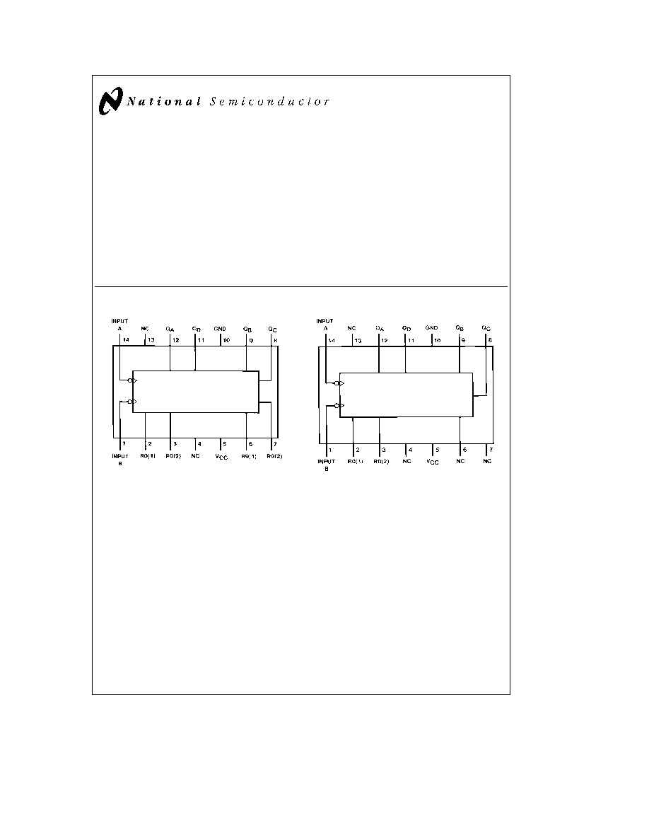
Connection Diagrams
(Dual-In-Line Packages)
TL F 6381 � 1
Order Number DM74LS90M or DM74LS90N
See NS Package Number M14A or N14A
TL F 6381 � 2
Order Number DM74LS93M or DM74LS93N
See NS Package Number M14A or N14A
C1995 National Semiconductor Corporation
RRD-B30M105 Printed in U S A
Absolute Maximum Ratings
(Note)
If Military Aerospace specified devices are required
please contact the National Semiconductor Sales
Office Distributors for availability and specifications
Supply Voltage
7V
Input Voltage (Reset)
7V
Input Voltage (A or B)
5 5V
Operating Free Air Temperature Range
DM74LS
0 C to
a
70 C
Storage Temperature Range
b
65 C to
a
150 C
Note
The ``Absolute Maximum Ratings'' are those values
beyond which the safety of the device cannot be guaran-
teed The device should not be operated at these limits The
parametric values defined in the ``Electrical Characteristics''
table are not guaranteed at the absolute maximum ratings
The ``Recommended Operating Conditions'' table will define
the conditions for actual device operation
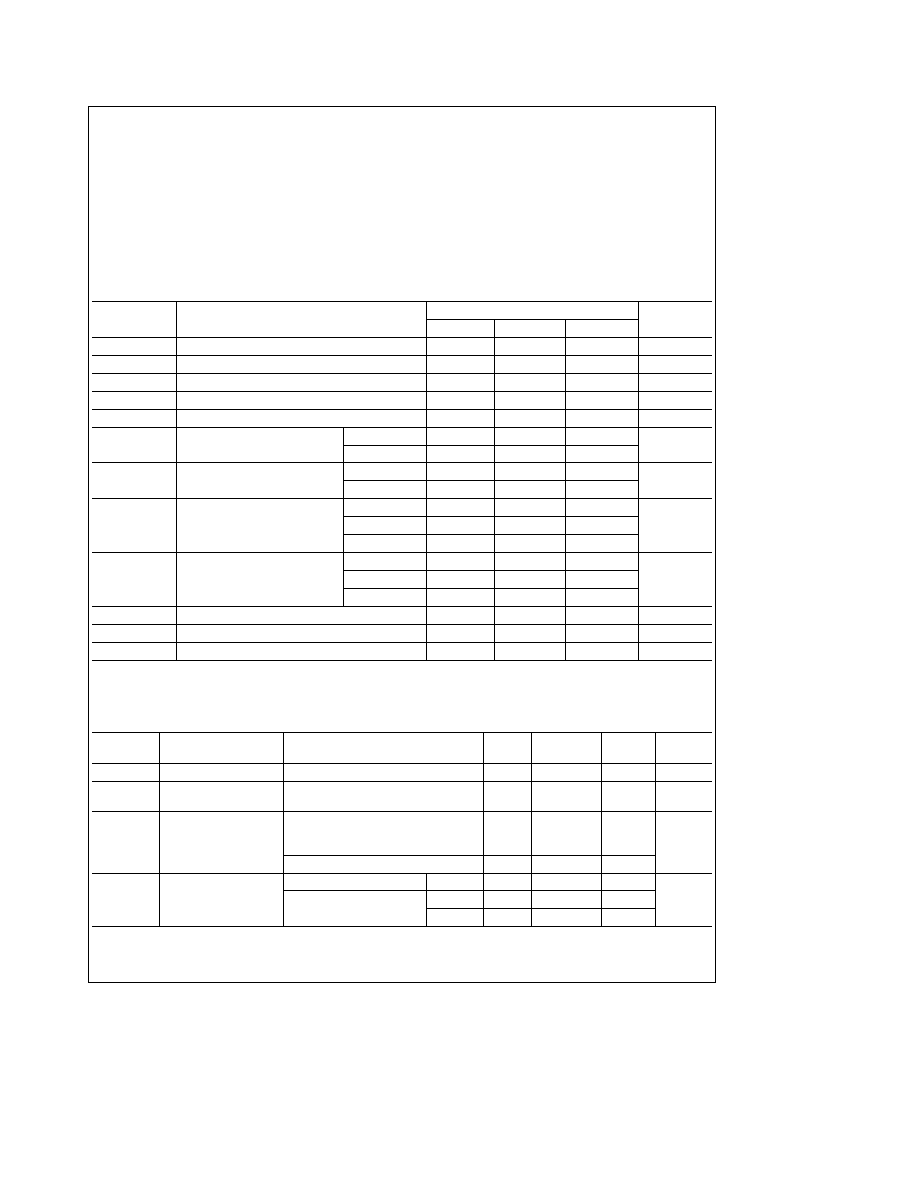
Recommended Operating Conditions
Symbol
Parameter
DM74LS90
Units
Min
Nom
Max
V
CC
Supply Voltage
4 75
5
5 25
V
V
IH
High Level Input Voltage
2
V
V
IL
Low Level Input Voltage
0 8
V
I
OH
High Level Output Current
b
0 4
mA
I
OL
Low Level Output Current
8
mA
f
CLK
Clock Frequency (Note 1)
A to Q
A
0
32
MHz
B to Q
B
0
16
f
CLK
Clock Frequency (Note 2)
A to Q
A
0
20
MHz
B to Q
B
0
10
t
W
Pulse Width (Note 1)
A
15
B
30
ns
Reset
15
t
W
Pulse Width (Note 2)
A
25
B
50
ns
Reset
25
t
REL
Reset Release Time (Note 1)
25
ns
t
REL
Reset Release Time (Note 2)
35
ns
T
A
Free Air Operating Temperature
0
70
C
Note 1
C
L
e
15 pF R
L
e
2 kX T
A
e
25 C and V
CC
e
5V
Note 2
C
L
e
50 pF R
L
e
2 kX T
A
e
25 C and V
CC
e
5V
'LS90 Electrical Characteristics
over recommended operating free air temperature range (unless otherwise noted)
Symbol
Parameter
Conditions
Min
Typ
Max
Units
(Note 1)
V
I
Input Clamp Voltage
V
CC
e
Min I
I
e b
18 mA
b
1 5
V
V
OH
High Level Output
V
CC
e
Min I
OH
e
Max
2 7
3 4
V
Voltage
V
IL
e
Max V
IH
e
Min
V
OL
Low Level Output
V
CC
e
Min I
OL
e
Max
Voltage
V
IL
e
Max V
IH
e
Min
0 35
0 5
V
(Note 4)
I
OL
e
4 mA V
CC
e
Min
0 25
0 4
I
I
Input Current
Max
V
CC
e
Max V
I
e
7V
Reset
0 1
Input Voltage
V
CC
e
Max
A
0 2
mA
V
I
e
5 5V
B
0 4
2
'LS90 Electrical Characteristics
over recommended operating free air temperature range (unless otherwise noted) (Continued)
Symbol
Parameter
Conditions
Min
Typ
Max
Units
(Note 1)
I
IH
High Level Input
V
CC
e
Max V
I
e
2 7V
Reset
20
Current
A
40
m
A
B
80
I
IL
Low Level Input
V
CC
e
Max V
I
e
0 4V
Reset
b
0 4
Current
A
b
2 4
mA
B
b
3 2
I
OS
Short Circuit
V
CC
e
Max (Note 2)
b
20
b
100
mA
Output Current
I
CC
Supply Current
V
CC
e
Max (Note 3)
9
15
mA
Note 1
All typicals are at V
CC
e
5V T
A
e
25 C
Note 2
Not more than one output should be shorted at a time and the duration should not exceed one second
Note 3
I
CC
is measured with all outputs open both RO inputs grounded following momentary connection to 4 5V and all other inputs grounded
Note 4
Q
A
outputs are tested at I
OL
e
Max plus the limit value of I
IL
for the B input This permits driving the B input while maintaining full fan-out capability
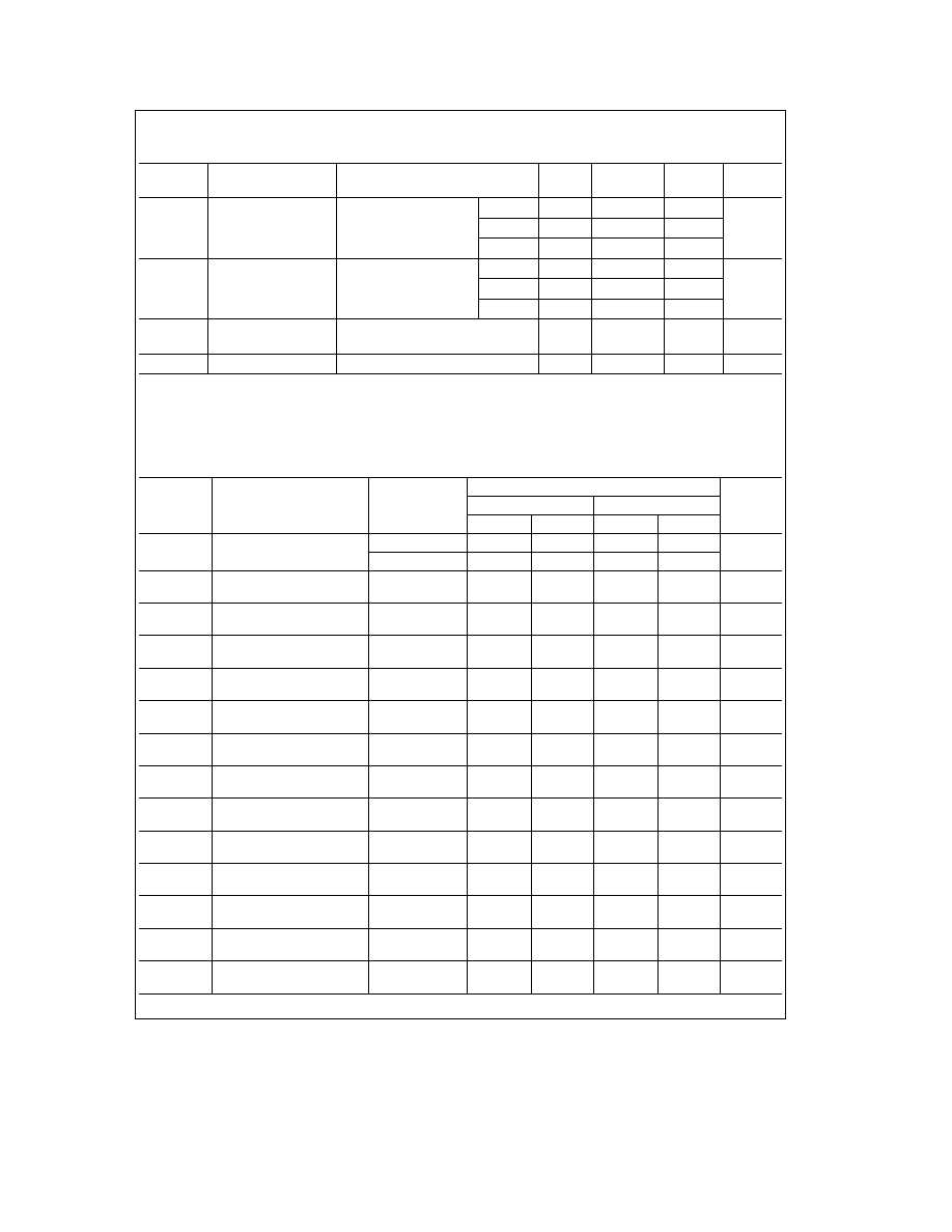
'LS90 Switching Characteristics
at V
CC
e
5V and T
A
e
25 C (See Section 1 for Test Waveforms and Output Load)
From (Input)
R
L
e
2 kX
Symbol
Parameter
To (Output)
C
L
e
15 pF
C
L
e
50 pF
Units
Min
Max
Min
Max
f
MAX
Maximum Clock
A to Q
A
32
20
MHz
Frequency
B to Q
B
16
10
t
PLH
Propagation Delay Time
A to Q
A
16
20
ns
Low to High Level Output
t
PHL
Propagation Delay Time
A to Q
A
18
24
ns
High to Low Level Output
t
PLH
Propagation Delay Time
A to Q
D
48
52
ns
Low to High Level Output
t
PHL
Propagation Delay Time
A to Q
D
50
60
ns
High to Low Level Output
t
PLH
Propagation Delay Time
B to Q
B
16
23
ns
Low to High Level Output
t
PHL
Propagation Delay Time
B to Q
B
21
30
ns
High to Low Level Output
t
PLH
Propagation Delay Time
B to Q
C
32
37
ns
Low to High Level Output
t
PHL
Propagation Delay Time
B to Q
C
35
44
ns
High to Low Level Output
t
PLH
Propagation Delay Time
B to Q
D
32
36
ns
Low to High Level Output
t
PHL
Propagation Delay Time
B to Q
D
35
44
ns
High to Low Level Output
t
PLH
Propagation Delay Time
SET-9 to
30
35
ns
Low to High Level Output
Q
A
Q
D
t
PHL
Propagation Delay Time
SET-9 to
40
48
ns
High to Low Level Output
Q
B
Q
C
t
PHL
Propagation Delay Time
SET-0 to
40
52
ns
High to Low Level Output
Any Q
3

Recommended Operating Conditions
Symbol
Parameter
DM74LS93
Units
Min
Nom
Max
V
CC
Supply Voltage
4 75
5
5 25
V
V
IH
High Level Input Voltage
2
V
V
IL
Low Level Input Voltage
0 8
V
I
OH
High Level Output Current
b
0 4
mA
I
OL
Low Level Output Current
8
mA
f
CLK
Clock Frequency (Note 1)
A to Q
A
0
32
B to Q
B
0
16
MHz
f
CLK
Clock Frequency (Note 2)
A to Q
A
0
20
B to Q
B
0
10
t
W
Pulse Width (Note 1)
A
15
B
30
ns
Reset
15
t
W
Pulse Width (Note 2)
A
25
B
50
ns
Reset
25
t
REL
Reset Release Time (Note 1)
25
ns
t
REL
Reset Release Time (Note 2)
35
ns
T
A
Free Air Operating Temperature
0
70
C
Note 1
C
L
e
15 pF R
L
e
2 kX T
A
e
25 C and V
CC
e
5V
Note 2
C
L
e
50 pF R
L
e
2 kX T
A
e
25 C and V
CC
e
5V
'LS93 Electrical Characteristics
over recommended operating free air temperature range (unless otherwise noted)
Symbol
Parameter
Conditions
Min
Typ
Max
Units
(Note 1)
V
I
Input Clamp Voltage
V
CC
e
Min I
I
e b
18 mA
b
1 5
V
V
OH
High Level Output
V
CC
e
Min I
OH
e
Max
2 7
3 4
V
Voltage
V
IL
e
Max V
IH
e
Min
V
OL
Low Level Output
V
CC
e
Min I
OL
e
Max
Voltage
V
IL
e
Max V
IH
e
Min
0 35
0 5
V
(Note 4)
I
OL
e
4 mA V
CC
e
Min
0 25
0 4
I
I
Input Current
Max
V
CC
e
Max V
I
e
7V
Reset
0 1
Input Voltage
V
CC
e
Max
A
0 2
mA
V
I
e
5 5V
B
0 4
I
IH
High Level Input
V
CC
e
Max
Reset
20
Current
V
I
e
2 7V
A
40
m
A
B
80
4
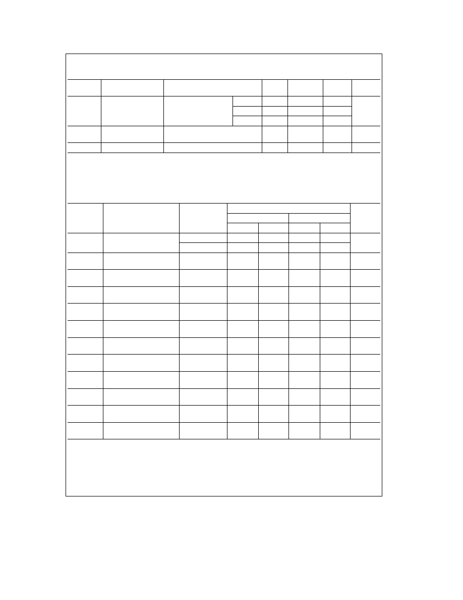
'LS93 Electrical Characteristics
over recommended operating free air temperature range (unless otherwise noted) (Continued)
Symbol
Parameter
Conditions
Min
Typ
Max
Units
(Note 1)
I
IL
Low Level Input
V
CC
e
Max V
I
e
0 4V
Reset
b
0 4
Current
A
b
2 4
mA
B
b
1 6
I
OS
Short Circuit
V
CC
e
Max (Note 2)
b
20
b
100
mA
Output Current
I
CC
Supply Current
V
CC
e
Max (Note 3)
9
15
mA
Note 1
All typicals are at V
CC
e
5V T
A
e
25 C
Note 2
Not more than one output should be shorted at a time and the duration should not exceed one second
Note 3
I
CC
is measured with all outputs open both RO inputs grounded following momentary connection to 4 5V and all other inputs grounded
Note 4
Q
A
outputs are tested at I
OL
e
max plus the limit value of I
IL
for the B input This permits driving the B input while maintaining full fan-out capability
'LS93 Switching Characteristics
at V
CC
e
5V and T
A
e
25 C (See Section 1 for Test Waveforms and Output Load)
From (Input)
R
L
e
2 kX
Symbol
Parameter
To (Output)
C
L
e
15 pF
C
L
e
50 pF
Units
Min
Max
Min
Max
f
MAX
Maximum Clock
A to Q
A
32
20
MHz
Frequency
B to Q
B
16
10
t
PLH
Propagation Delay Time
A to Q
A
16
20
ns
Low to High Level Output
t
PHL
Propagation Delay Time
A to Q
A
18
24
ns
High to Low Level Output
t
PLH
Propagation Delay Time
A to Q
D
70
85
ns
Low to High Level Output
t
PHL
Propagation Delay Time
A to Q
D
70
90
ns
High to Low Level Output
t
PLH
Propagation Delay Time
B to Q
B
16
23
ns
Low to High Level Output
t
PHL
Propagation Delay Time
B to Q
B
21
30
ns
High to Low Level Output
t
PLH
Propagation Delay Time
B to Q
C
32
37
ns
Low to High Level Output
t
PHL
Propagation Delay Time
B to Q
C
35
44
ns
High to Low Level Output
t
PLH
Propagation Delay Time
B to Q
D
51
60
ns
Low to High Level Output
t
PHL
Propagation Delay Time
B to Q
D
51
70
ns
High to Low Level Output
t
PHL
Propagation Delay Time
SET-0 to
40
52
ns
High to Low Level Output
Any Q
5