
TL F 6353
54LS14DM74LS14
Hex
Inverters
with
Schmitt
Trigger
Inputs
June 1989
54LS14 DM74LS14 Hex Inverters
with Schmitt Trigger Inputs
General Description
This device contains six independent gates each of which
performs the logic INVERT function Each input has hyster-
esis which increases the noise immunity and transforms a
slowly changing input signal to a fast changing jitter free
output
Connection Diagram
Dual-In-Line Package
TL F 6353 ≠ 1
Order Number 54LS14DMQB 54LS14FMQB
54LS14LMQB DM74LS14M or DM74LS14N
See NS Package Number E20A J14A M14A N14A or W14B
Function Table
Y
e
A
Input
Output
A
Y
L
H
H
L
H
e
High Logic Level
L
e
Low Logic Level
C1995 National Semiconductor Corporation
RRD-B30M105 Printed in U S A
Absolute Maximum Ratings
(Note)
If Military Aerospace specified devices are required
please contact the National Semiconductor Sales
Office Distributors for availability and specifications
Supply Voltage
7V
Input Voltage
7V
Operating Free Air Temperature Range
54LS
b
55 C to
a
125 C
DM74LS
0 C to
a
70 C
Storage Temperature Range
b
65 C to
a
150 C
Note
The ``Absolute Maximum Ratings'' are those values
beyond which the safety of the device cannot be guaran-
teed The device should not be operated at these limits The
parametric values defined in the ``Electrical Characteristics''
table are not guaranteed at the absolute maximum ratings
The ``Recommended Operating Conditions'' table will define
the conditions for actual device operation
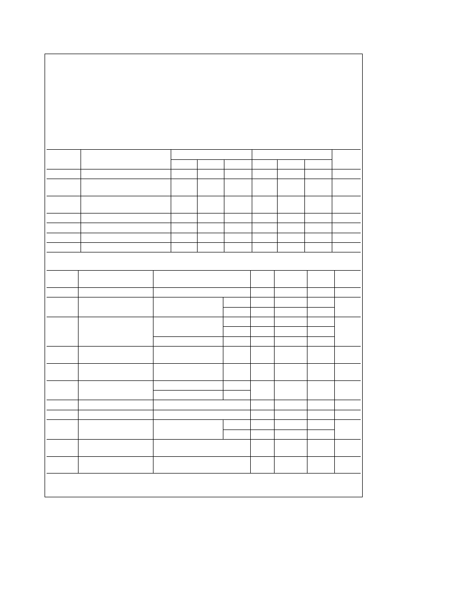
Recommended Operating Conditions
Symbol
Parameter
54LS14
DM74LS14
Units
Min
Nom
Max
Min
Nom
Max
V
CC
Supply Voltage
4 5
5
5 5
4 75
5
5 25
V
V
Ta
Positive-Going Input
1 5
1 6
2 0
1 4
1 6
1 9
V
Threshold Voltage (Note 1)
V
Tb
Negative-Going Input
0 6
0 8
1 1
0 5
0 8
1
V
Threshold Voltage (Note 1)
HYS
Input Hysteresis (Note 1)
0 4
0 8
0 4
0 8
V
I
OH
High Level Output Current
b
0 4
b
0 4
mA
I
OL
Low Level Output Current
4
8
mA
T
A
Free Air Operating Temperature
b
55
125
0
70
C
Electrical Characteristics
over recommended operating free air temperature range (unless otherwise noted)
Symbol
Parameter
Conditions
Min
Typ
Max
Units
(Note 2)
V
I
Input Clamp Voltage
V
CC
e
Min I
I
e b
18 mA
b
1 5
V
V
OH
High Level Output
V
CC
e
Min I
OH
e
Max
54LS
2 5
3 4
V
Voltage
V
IL
e
Max
DM74
2 7
3 4
V
OL
Low Level Output
V
CC
e
Min I
OL
e
Max
54LS
0 25
0 4
Voltage
V
IH
e
Min
DM74
0 35
0 5
V
V
CC
e
Min I
OL
e
4 mA
DM74
0 25
0 4
I
Ta
Input Current at
V
CC
e
5V V
I
e
V
Ta
DM74
b
0 14
mA
Positive-Going Threshold
I
Tb
Input Current at
V
CC
e
5V V
I
e
V
Tb
DM74
b
0 18
mA
Negative-Going Threshold
I
I
Input Current
Max
V
CC
e
Max V
I
e
7V
DM74
0 1
mA
Input Voltage
V
CC
e
Max V
I
e
10 0V
54LS
I
IH
High Level Input Current
V
CC
e
Max V
I
e
2 7V
20
m
A
I
IL
Low Level Input Current
V
CC
e
Max V
I
e
0 4V
b
0 4
mA
I
OS
Short Circuit
V
CC
e
Max
54LS
b
20
b
100
mA
Output Current
(Note 3)
DM74
b
20
b
100
I
CCH
Supply Current with
V
CC
e
Max
8 6
16
mA
Outputs High
I
CCL
Supply Current with
V
CC
e
Max
12
21
mA
Outputs Low
Note 1
V
CC
e
5V
Note 2
All typicals are at V
CC
e
5V T
A
e
25 C
Note 3
Not more than one output should be shorted at a time and the duration should not exceed one second
2

Physical Dimensions
inches (millimeters) (Continued)
14-Lead Small Outline Molded Package (M)
Order Number DM74LS14M
NS Package Number M14A
14-Lead Molded Dual-In-Line Package (N)
Order Number DM74LS14N
NS Package Number N14A
5

