 | –≠–ª–µ–∫—Ç—Ä–æ–Ω–Ω—ã–π –∫–æ–º–ø–æ–Ω–µ–Ω—Ç: 74LVT2244 | –°–∫–∞—á–∞—Ç—å:  PDF PDF  ZIP ZIP |
TL F 12170
74LVT2244
33V
ABT
Octal
BufferLine
Driver
with
TRI-STATE
Outputs
ADVANCE INFORMATION
December 1996
74LVT2244
3 3V ABT Octal Buffer Line Driver
with TRI-STATE
Outputs
General Description
The LVT2244 is an octal buffer and line driver designed to
be employed as a memory address driver clock driver and
bus oriented transmitter or receiver which provides im-
proved PC board density The equivalent 25X-Series resis-
tor helps reduce output overshoot and undershoot
These octal buffers and line drivers are designed for low-
voltage (3 3V) V
CC
applications but with the capability to
provide a TTL interface to a 5V environment The LVT2244
is fabricated with an advanced BiCMOS technology to
achieve high speed operation similar to 5V ABT while main-
taining a low power dissipation
Features
Y
Input and output interface capability to systems at 5V
V
CC
Y
Bus-Hold data inputs eliminate the need for external
pull-up resistors to hold unused inputs
Y
Equivalent 25X-Series resistor on outputs
Y
Live insertion extraction permitted
Y
Power Up Down high impedance provides glitch-free
bus loading
Y
Outputs source sink
b
12 mA
a
12 mA
Y
Available in SOIC JEDEC
SOIC EIAJ
TSSOP and
SSOPII
Y
Latch-up performance exceeds 500 mA
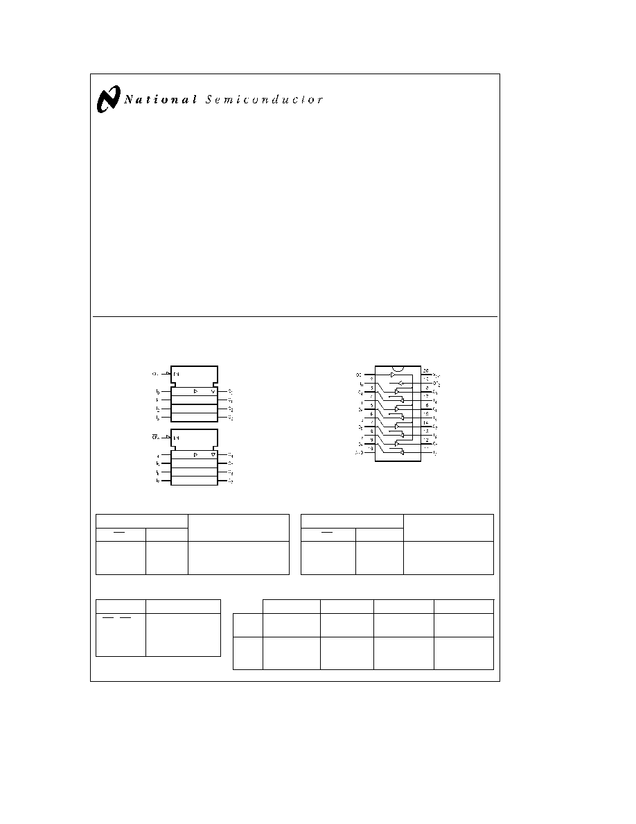
Logic Symbol
IEEE IEC
TL F 12170 ≠ 1
Connection Diagram
Pin Assignment
for SOIC TSSOP and SSOPII
TL F 12170 ≠ 2
Truth Tables
Inputs
Outputs
OE
1
I
n
(Pins 12 14 16 18)
L
L
L
L
H
H
H
X
Z
Inputs
Outputs
OE
2
I
n
(Pins 3 5 7 9)
L
L
L
L
H
H
H
X
Z
H
e
HIGH Voltage Level
L
e
LOW Voltage Level
X
e
Immaterial
Z
e
High Impedance
Pin Names
Description
OE
1
OE
2
TRI-STATE Output
Enable Inputs
I
0
≠ I
7
Inputs
O
0
≠ O
7
Outputs
SOIC JEDEC
SOIC EIAJ
TSSOP JEDEC
SSOPII
Order
74LVT2244WM
74LVT2244SJ
74LVT2244MTC
74LVT2244MSA
Number 74LVT2244WMX 74LVT2244SJX 74LVT2244MTCX 74LVT2244MSAX
See NS
M20B
M20D
MTC20
MSA20
Package
Number
TRI-STATE
is a registered trademark of National Semiconductor Corporation
C1996 National Semiconductor Corporation
RRD-B30M17 Printed in U S A
http
www national com

Absolute Maximum Ratings
(Note 1)
Symbol
Parameter
Value
Conditions
Units
V
CC
Supply Voltage
b
0 5 to
a
7 0
V
V
I
DC Input Voltage
b
0 5 to
a
7 0
V
V
O
DC Output Voltage
b
0 5 to
a
7 0
Output in TRI-STATE
V
b
0 5 to
a
7 0
Output in High or Low State (Note 2)
V
I
IK
DC Input Diode Current
b
50
V
I
k
GND
mA
I
OK
DC Output Diode Current
b
50
V
O
k
GND
mA
I
O
DC Output Current
64
V
O
l
V
CC
Output at High State
mA
128
V
O
l
V
CC
Output at Low State
I
CC
DC Supply Current per Supply Pin
g
64
mA
I
GND
DC Ground Current per Ground Pin
g
128
mA
T
STG
Storage Temperature
b
65 to
a
150
C
Note 1
The Absolute Maximum Ratings are those values beyond which the safety of the device cannot be guaranteed The device should not be operated at these
limits The parametric values defined in the ``Electrical Characteristics'' table are not guaranteed at the Absolute Maximum Ratings The ``Recommended Operating
Conditions'' table will define the conditions for actual device operation
Note 2
I
O
Absolute Maximum Rating must be observed
Recommended Operating Conditions
Symbol
Parameter
Min
Max
Units
V
CC
Supply Voltage
Operating
2 0
3 6
V
Data Retention
1 5
3 6
V
I
Input Voltage
0
3 6
V
V
O
Output Voltage
HIGH or LOW State
0
V
CC
V
TRI-STATE
0
5 5
I
OH
High-Level Output Current
b
12
mA
I
OL
Low-Level Output Current
12
T
A
Free-Air Operating Temperature
b
40
85
C
D
t DV
Input Edge Rate V
IN
e
0 8V ≠ 2 0V V
CC
e
3 0V
0
10
ns V
DC Electrical Characteristics
Symbol
Parameter
V
CC
(V)
T
A
e b
40 C to
a
85 C
Units
Conditions
Min
Typ
Max
(Note 3)
V
IK
Input Clamp Diode Voltage
2 7
b
1 2
V
I
I
e b
18 mA
V
IH
Input HIGH Voltage
2 7 ≠ 3 6
2 0
V
V
O
s
0 1V or
V
O
t
V
CC
b
0 1V
V
IL
Input LOW Voltage
2 7 ≠ 3 6
0 8
V
OH
Output HIGH Voltage
2 7 ≠ 3 6
V
CC
b
0 2
V
I
OH
e b
100 mA
3 0
2 0
V
I
OH
e b
12 mA
V
OL
Output LOW Voltage
2 7
0 2
V
I
OL
e
100 mA
3 0
0 8
V
I
OL
e
12 mA
http
www national com
2
DC Electrical Characteristics
(Continued)
Symbol
Parameter
V
CC
(V)
T
A
e b
40 C to
a
85 C
Units
Conditions
Min
Typ
Max
(Note 3)
I
I(HOLD)
Bus-Hold Input Minimum Drive
3 0
75
m
A
V
I
e
0 8V
b
75
m
A
V
I
e
2 0V
I
I(OD)
Current to Change State
Bus-Hold Input Over-Drive
3 0
500
m
A
(Note 4)
b
500
m
A
(Note 5)
I
I
Input Current
3 6
10
m
A
V
I
e
5 5V
Control Pins
3 6
g
1
m
A
V
I
e
0V or V
CC
Data Pins
3 6
b
5
m
A
V
I
e
0V
1
m
A
V
I
e
V
CC
I
OFF
Power Off Leakage Current
0
g
100
m
A
0V
s
V
I
or V
O
s
5 5V
I
PU PD
Power up down TRI-STATE
0 ≠ 1 2V
g
100
m
A
V
O
e
0 5V to V
CC
(Note 6)
Output Current
V
I
e
GND or V
CC
I
OZL
TRI-STATE Output Leakage Current
3 6
b
5
m
A
V
O
e
0 5V
I
OZH
TRI-STATE Output Leakage Current
3 6
5
m
A
V
O
e
3 0V
I
OZH
a
TRI-STATE Output Leakage Current
3 6
10
m
A
V
CC
k
V
O
s
5 5V
I
CCH
Power Supply Current
3 6
0 19
mA
Outputs High
I
CCL
Power Supply Current
3 6
12
mA
Outputs Low
I
CCZ
Power Supply Current
3 6
0 19
mA
Outputs Disabled
I
CCZ
a
Power Supply Current
3 6
0 19
mA
V
CC
s
V
O
s
5 5V
Outputs Disabled
D
I
CC
Increase in Power Supply Current
3 6
0 2
mA
One Input at V
CC
b
0 6V
(Note 7)
Other Inputs at V
CC
or GND
Note 3
All typical values are at V
CC
e
3 3V T
A
e
25 C
Note 4
An external driver must source at least the specified current to switch from LOW to HIGH
Note 5
An external driver must sink at least the specified current to switch from HIGH to LOW
Note 6
This parameter is valid for any V
CC
between 0V and 1 2V at 25 C only
Note 7
This is the increase in supply current for each input that is at the specified voltage level rather than V
CC
or GND
Dynamic Switching Characteristics
(Note 8)
Symbol
Parameter
V
CC
(V)
T
A
e
25 C
Units
C
L
e
50 pF R
L
e
500X
Conditions
Min
Typ
Max
V
OLP
Quiet Output Maximum Dynamic V
OL
3 3
0 8
V
(Note 9)
V
OLV
Quiet Output Minimum Dynamic V
OL
3 3
b
0 8
V
(Note 9)
Note 8
Characterized in SOIC package Guaranteed parameter but not tested
Note 9
Max number of outputs defined as (n) n
b
1 data inputs are driven 0V to 3V Output under test held LOW
http
www national com
3

AC Electrical Characteristics
Symbol
Parameter
T
A
e b
40 C to
a
85 C
Units
C
L
e
50 pF R
L
e
500X
V
CC
e
3 3V
g
0 3V
V
CC
e
2 7V
Min
Typ
Max
Min
Max
(Note 3)
t
PLH
Propagation Delay Data to Output
1 0
4 1
1 0
5 0
ns
t
PHL
1 0
4 1
1 0
5 2
t
PZH
Output Enable Time
1 0
5 2
1 0
6 3
ns
t
PZL
1 0
5 2
1 0
6 7
t
PHZ
Output Disable Time
1 8
5 6
1 8
6 3
ns
t
PLZ
1 8
5 1
1 8
5 6
t
OSHL
Output to Output Skew
1 0
ns
t
OSLH
(Note 10)
Note 3
All typical values are at V
CC
e
3 3V T
A
e
25 C
Note 10
Skew is defined as the absolute value of the difference between the actual propagation delay for any two separate outputs of the same device The
specification applies to any outputs switching in the same direction either HIGH to LOW (t
OSHL
) or LOW to HIGH (t
OSLH
) Parameter guaranteed by design
Capacitance
(Note 11)
Symbol
Parameter
Min
Typ
Max
Units
Conditions
C
IN
Input Capacitance
4
pF
V
CC
e
0V V
I
e
0V or V
CC
C
OUT
Output Capacitance
8
pF
V
CC
e
3 0V V
O
e
0V or V
CC
Note 11
Capacitance is measured at frequency f
e
1 MHz per MIL-STD-883B Method 3012
74LVT2244 Ordering Information
The device number is used to form part of a simplified purchasing code where the package type and temperature range are
defined as follows
TL F 12170 ≠ 3
http
www national com
4

Physical Dimensions
inches (millimeters) unless otherwise noted
20-Lead (0 300 Wide) Molded Small Outline Package JEDEC
Order Number 74LVT2244WM or 74LVT2244WMX
NS Package Number M20B
http
www national com
5