
TL F 11540
74LVX4245
8-Bit
Dual
Supply
Translating
Transceiver
with
TRI-STATE
Outputs
October 1995
74LVX4245
8-Bit Dual Supply Translating Transceiver
with TRI-STATE
Outputs
General Description
The LVX4245 is a dual-supply 8-bit translating transceiver
that is designed to interface between a 5V bus and a 3V bus
in a mixed 3V 5V supply environment The Transmit Re-
ceive (T R) input determines the direction of data flow
Transmit (active-HIGH) enables data from A ports to B
ports Receive (active-LOW) enables data from B ports to A
ports The Output Enable input when HIGH disables both A
and B ports by placing them in a HIGH Z condition The A
port interfaces with the 5V bus the B port interfaces with
the 3V bus
The LVX4245 is suitable for mixed voltage applications such
as laptop computers using 3 3V CPU's and 5V LCD dis-
plays
Features
Y
Bidirectional interface between 5V and 3V buses
Y
Control inputs compatible with TTL level
Y
5V data flow at A port and 3V data flow at B port
Y
Outputs source sink 24 mA at 5V bus 12 mA at 3V
bus
Y
Guaranteed simultaneous switching noise level and dy-
namic threshold performance
Y
Available in SOIC QSOP and TSSOP packages
Y
Implements patented Quiet Series EMI reduction
circuitry
Y
Functionally compatible with the 74 series 245
Logic Symbol
TL F 11540 ≠ 1
Pin Names
Description
OE
Output Enable Input
T R
Transmit Receive Input
A
0
≠ A
7
Side A Inputs or TRI-STATE Outputs
B
0
≠ B
7
Side B Inputs or TRI-STATE Outputs
Connection Diagram
Pin Assignment
for SOIC QSOP and TSSOP
TL F 11540 ≠ 2
SOIC JEDEC
QSOP
TSSOP
Order Number
74LVX4245WM
74LVX4245QSC
74LVX4245MTC
74LVX4245WMX
74LVX4245QSCX
74LVX4245MTCX
See NS Package Number
M24B
MQA24
MTC24
TRI-STATE
is a registered trademark of National Semiconductor Corporation
C1995 National Semiconductor Corporation
RRD-B30M115 Printed in U S A
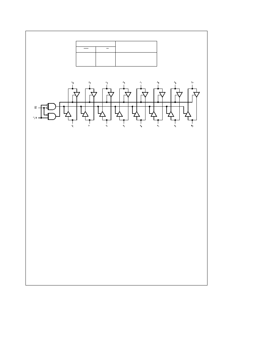
Truth Table
Inputs
Outputs
OE
T R
L
L
Bus B Data to Bus A
L
H
Bus A Data to Bus B
H
X
HIGH-Z State
Logic Diagram
TL F 11540 ≠ 6
2

Absolute Maximum Ratings
(Note)
If Military Aerospace specified devices are required
please contact the National Semiconductor Sales
Office Distributors for availability and specifications
Supply Voltage (V
CCA
V
CCB
)
b
0 5V to
a
7 0V
DC Input Voltage (V
I
)
OE T R
b
0 5V to V
CCA
a
0 5V
DC Input Output Voltage (V
I O
)
A(n)
b
0 5V to V
CCA
a
0 5V
B(n)
b
0 5V to V
CCB
a
0 5V
DC Input Diode Current (I
IN
)
OE T R
g
20 mA
DC Output Diode Current (I
OK
)
g
50 mA
DC Output Source or Sink Current (I
O
)
g
50 mA
DC V
CC
or Ground Current
per Output Pin (I
CC
or I
GND
)
g
50 mA
and Max Current
I
CCA
g
200 mA
I
CCB
g
100 mA
Storage Temperature Range (T
STG
)
b
65 C to
a
150 C
DC Latch-Up Source or Sink Current
g
300 mA
Note
The ``Absolute Maximum Ratings'' are those values
beyond which the safety of the device cannot be guaran-
teed The device should not be operated at these limits The
parametric values defined in the ``Electrical Characteristics''
table are not guaranteed at the absolute maximum ratings
The ``Recommended Operating Conditions'' table will define
the conditions for actual device operation
Recommended Operating
Conditions
Supply Voltage
V
CCA
4 5V to 5 5V
V
CCB
2 7V to 3 6V
Input Voltage (V
I
)
OE T R
0V to V
CCA
Input Output Voltage (V
I O
)
A(n)
0V to V
CCA
B(n)
0V to V
CCB
Free Air Operating Temperature (T
A
)
74LVX
b
40 C to
a
85 C
Minimum Input Edge Rate (Dt DV)
8 ns V
V
IN
from 30% to 70% of V
CC
V
CC
3 0V 4 5V 5 5V
DC Electrical Characteristics
Symbol
Parameter
V
CCA
(V)
V
CCB
(V)
74LVX4245
74LVX4245
Units
Conditions
T
A
a
25 C
T
A
e b
40 C
to
a
85 C
Typ
Guaranteed Limits
V
IHA
Minimum
A(n) T R
5 5
3 3
2 0
2 0
V
V
OUT
s
0 1V or
High Level
OE
4 5
3 3
2 0
2 0
t
V
CC
b
0 1V
V
IHB
Input Voltage
B(n)
5 0
3 6
2 0
2 0
5 0
2 7
2 0
2 0
V
ILA
Maximum Low Level
A(n) T R
5 5
3 3
0 8
0 8
V
V
OUT
s
0 1V or
Input Voltage
OE
4 5
3 3
0 8
0 8
t
V
CC
b
0 1V
V
ILB
B(n)
5 0
2 7
0 8
0 8
5 0
3 6
0 8
0 8
V
OHA
Minimum High Level
4 5
3 0
4 5
4 4
4 4
V
I
OUT
e b
100 mA
Output Voltage
4 5
3 0
4 25
3 86
3 76
I
OH
e b
24 mA
V
OHB
4 5
3 0
2 99
2 9
2 9
V
I
OUT
e b
100 mA
4 5
3 0
2 8
2 4
2 4
I
OH
e b
12 mA
4 5
2 7
2 5
2 4
2 4
I
OL
e b
8 mA
V
OLA
Maximum Low Level
4 5
3 0
0 002
0 1
0 1
V
I
OUT
e
100 mA
Output Voltage
4 5
3 0
0 18
0 36
0 44
I
OL
e
24 mA
V
OLB
4 5
3 0
0 002
0 1
0 1
I
OUT
e
100 mA
4 5
3 0
0 1
0 31
0 4
V
I
OL
e
12 mA
4 5
2 7
0 1
0 31
0 4
I
OL
e
8 mA
I
IN
Maximum Input
V
I
e
V
CCA
GND
Leakage Current
5 5
3 6
g
0 1
g
1 0
m
A
OE T R
I
OZA
Maximum TRI-STATE
V
I
e
V
IL
V
IH
Output Leakage
5 5
3 6
g
0 5
g
5 0
m
A
OE
e
V
CCA
A(n)
V
O
e
V
CCA
GND
3

DC Electrical Characteristics
(Continued)
Symbol
Parameter
V
CCA
(V)
V
CCB
(V)
74LVX4245
74LVX4245
Units
Conditions
T
A
e a
25 C
T
A
e b
40 C
to
a
85 C
Typ
Guaranteed Limits
I
OZB
Maximum TRI-STATE
V
I
e
V
IL
V
IH
Output Leakage
5 5
3 6
g
0 5
g
5 0
m
A
OE
e
V
CCA
B(n)
V
O
e
V
CCB
GND
D
I
CC
Maximum I
CCT
Input
5 5
3 6
1 0
1 35
1 5
mA
V
I
e
V
CCA
b
2 1V
A(n) T R OE
Input
B(n)
5 5
3 6
0 35
0 5
mA
V
I
e
V
CCB
b
0 6V
I
CCA
Quiescent V
CCA
A(n)
e
V
CCA
or GND
Supply Current
5 5
3 6
8
80
m
A
B(n)
e
V
CCB
or GND
OE
e
GND T R
e
GND
I
CCB
Quiescent V
CCB
A(n)
e
V
CCA
or GND
Supply Current
5 5
3 6
5
50
m
A
B(n)
e
V
CCB
or GND
OE
e
GND T R
e
V
CCA
V
OLPA
Quiet Output Maximum
5 0
3 3
1 5
V
(Notes 1 2)
V
OLPB
Dynamic V
OL
5 0
3 3
0 8
V
OLVA
Quiet Output Minimum
5 0
3 3
b
1 2
V
(Notes 1 2)
V
OLVB
Dynamic V
OL
5 0
3 3
b
0 8
V
IHDA
Minimum High Level
5 0
3 3
2 0
V
(Notes 1 3)
V
IHDB
Dynamic Input Voltage
5 0
3 3
2 0
V
ILDA
Maximum Low Level
5 0
3 3
0 8
V
(Notes 1 3)
V
ILDB
Dynamic Input Voltage
5 0
3 3
0 8
Maximum test duration 2 0 ms one output loaded at a time
Note 1
Worst case package
Note 2
Max number of outputs defined as (n) Data inputs are driven 0V to V
CC
level one output at GND
Note 3
Max number of Data Inputs (n) switching (n
b
1) inputs switching 0V to V
CC
level Input-under-test switching V
CC
level to threshold (V
IHD
) OV to threshold
(V
ILD
) f
e
1 MHz
4

AC Electrical Characteristics
Symbol
Parameters
74LVX4245
74LVX4245
74LVX4245
Units
T
A
e a
25 C
T
A
e b
40 C to
a
85 C
T
A
e b
40 C to
a
85 C
C
L
e
50 pF
C
L
e
50 pF
C
L
e
50 pF
V
CCA
e
5V
V
CCA
e
5V
V
CCA
e
5V
V
CCB
e
3 3V
V
CCB
e
3 3V
V
CCB
e
2 7V
Min
Typ
Max
Min
Max
Min
Max
t
PHL
Propagation Delay
1 0
5 1
8 5
1 0
9 0
1 0
10 0
ns
t
PLH
A to B
1 0
5 3
8 5
1 0
9 0
1 0
10 0
t
PHL
Propagation Delay
1 0
5 4
8 5
1 0
9 0
1 0
10 0
ns
t
PLH
B to A
1 0
5 5
8 5
1 0
9 0
1 0
10 0
t
PZL
Output Enable Time
1 0
6 5
10 0
1 0
10 5
1 0
11 5
ns
t
PZH
OE to B
1 0
6 7
10 0
1 0
10 5
1 0
11 5
t
PZL
Output Enable Time
1 0
5 2
9 0
1 0
9 5
1 0
10 0
ns
t
PZH
OE to A
1 0
5 8
9 0
1 0
9 5
1 0
10 0
t
PHZ
Output Disable Time
1 0
6 0
9 5
1 0
10 0
1 0
10 0
ns
t
PLZ
OE to B
1 0
3 3
6 5
1 0
7 0
1 0
7 5
t
PHZ
Output Disable Time
1 0
3 9
7 0
1 0
7 5
1 0
7 5
ns
t
PLZ
OE to A
1 0
2 9
6 5
1 0
7 0
1 0
7 5
t
OSHL
Output to Output
t
OSLH
Skew
1 0
1 5
1 5
1 5
ns
Data to Output
Voltage Range 5 0V is 5 0V
g
0 5V
Voltage Range 3 3V is 3 3V
g
0 3V
Skew is defined as the absolute value of the difference between the actual propagation delay for any two separate outputs of the same device The
specification applies to any outputs switching in the same direction either HIGH to LOW (t
OSHL
) or LOW to HIGH (t
OSLH
) Parameter guaranteed by
design
Capacitance
Symbol
Parameter
Typ
Units
Conditions
C
IN
Input Capacitance
4 5
pF
V
CC
e
Open
C
I O
Input Output
15
pF
V
CCA
e
5 0V
Capacitance
V
CCB
e
3 3V
C
PD
Power Dissipation
B
x
A
55
pF
V
CCA
e
5 0V
Capacitance
A
x
B
40
pF
V
CCB
e
3 3V
C
PD
is measured at 10 MHz
8-Bit Dual Supply Translating Transceiver
The LVX4245 is a dual supply device capable of bidirection-
al signal translation This level shifting ability provides an
efficient interface between low voltage CPU local bus with
memory and a standard bus defined by 5V I O levels The
device control inputs can be controlled by either the low
voltage CPU and core logic or a bus arbitrator with 5V I O
levels
Manufactured on a sub-micron CMOS process
the
LVX4245 is ideal for mixed voltage applications such as
notebook computers using 3 3V CPU's and 5V peripheral
devices
TL F 11540 ≠ 3
5