 | –≠–ª–µ–∫—Ç—Ä–æ–Ω–Ω—ã–π –∫–æ–º–ø–æ–Ω–µ–Ω—Ç: 9324FMQB | –°–∫–∞—á–∞—Ç—å:  PDF PDF  ZIP ZIP |
TL F 9792
9324DM9324
5-Bit
Comparator
June 1989
9324 DM9324 5-Bit Comparator
General Description
The 9324 expandable comparators provide comparison be-
tween two 5-bit words and give three outputs
``less than''
``greater than'' and ``equal to'' A HIGH on the active LOW
Enable Input forces all three outputs LOW
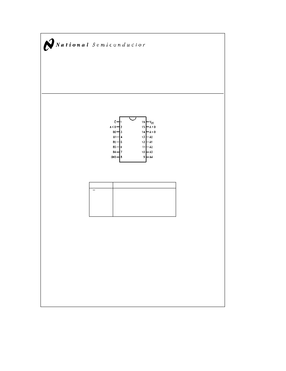
Connection Diagram
Dual-In-Line Package
TL F 9792 ≠ 1
Order Number 9324DMQB 9324FMQB or DM9324N
See NS Package Number J16A N16E or W16A
Pin Names
Description
E
Enable Input (Active LOW)
A0 ≠ A4
Word A Parallel Inputs
B0 ≠ B4
Word B Parallel Inputs
A
k
B
A Less than B Output (Active HIGH)
A
l
B
A Greater than B Output (Active HIGH)
A
e
B
A Equal to B Output (Active HIGH)
C1995 National Semiconductor Corporation
RRD-B30M115 Printed in U S A

Absolute Maximum Ratings
(Note)
If Military Aerospace specified devices are required
please contact the National Semiconductor Sales
Office Distributors for availability and specifications
Supply Voltage
7V
Input Voltage
5 5V
Operating Free Air Temperature Range
Military
b
55 C to
a
125 C
Commercial
0 C to
a
70 C
Storage Temperature Range
b
65 C to
a
150 C
Note
The ``Absolute Maximum Ratings'' are those values
beyond which the safety of the device cannot be guaran-
teed The device should not be operated at these limits The
parametric values defined in the ``Electrical Characteristics''
table are not guaranteed at the absolute maximum ratings
The ``Recommended Operating Conditions'' table will define
the conditions for actual device operation
Recommended Operating Conditions
Symbol
Parameter
Military
Commercial
Units
Min
Nom
Max
Min
Nom
Max
V
CC
Supply Voltage
4 5
5
5 5
4 75
5
5 25
V
V
IH
High Level Input Voltage
2
2
V
V
IL
Low Level Input Voltage
0 8
0 8
V
I
OH
High Level Output Current
b
0 8
b
0 8
mA
I
OL
Low Level Output Current
16
16
mA
T
A
Free Air Operating Temperature
b
55
125
0
70
C
Electrical Characteristics
Over recommended operating free air temperature range (unless otherwise noted)
Symbol
Parameter
Conditions
Min
Typ
Max
Units
(Note 1)
V
I
Input Clamp Voltage
V
CC
e
Min I
I
e b
12 mA
b
1 5
V
V
OH
High Level Output Voltage
V
CC
e
Min I
OH
e
Max
2 4
3 4
V
V
IL
e
Max
V
OL
Low Level Output Voltage
V
CC
e
Min I
OL
e
Max
0 2
0 4
V
V
IH
e
Min
I
I
Input Current
Max
V
CC
e
Max V
I
e
5 5V
1
mA
Input Voltage
I
IH
High Level Input Current
V
CC
e
Max V
I
e
2 4V
80
m
A
I
IL
Low Level Input Current
V
CC
e
Max V
I
e
0 4V
b
3 2
mA
I
OS
Short Circuit
V
CC
e
Max
MIL
b
20
b
70
mA
Output Current
(Note 2)
COM
b
20
b
70
I
CC
Supply Current
V
CC
e
Max
81
mA
Note 1
All typicals are at V
CC
e
5V T
A
e
25 C
Note 2
Not more than one output should be shorted at a time
2
Switching Characteristics
V
CC
e a
5 0V T
A
e a
25 C (See Section 1 for waveforms and load configurations)
Symbol
Parameter
C
L
e
15 pF
Units
Min
Max
t
PLH
Propagation Delay
14
ns
t
PHL
E to A
e
B
14
t
PLH
Propagation Delay
25
ns
t
PHL
A
n
B
n
to A
l
B
22
t
PLH
Propagation Delay
26
ns
t
PHL
A
n
B
n
to A
k
B
21
t
PLH
Propagation Delay
30
ns
t
PHL
A
n
B
n
to A
e
B
32
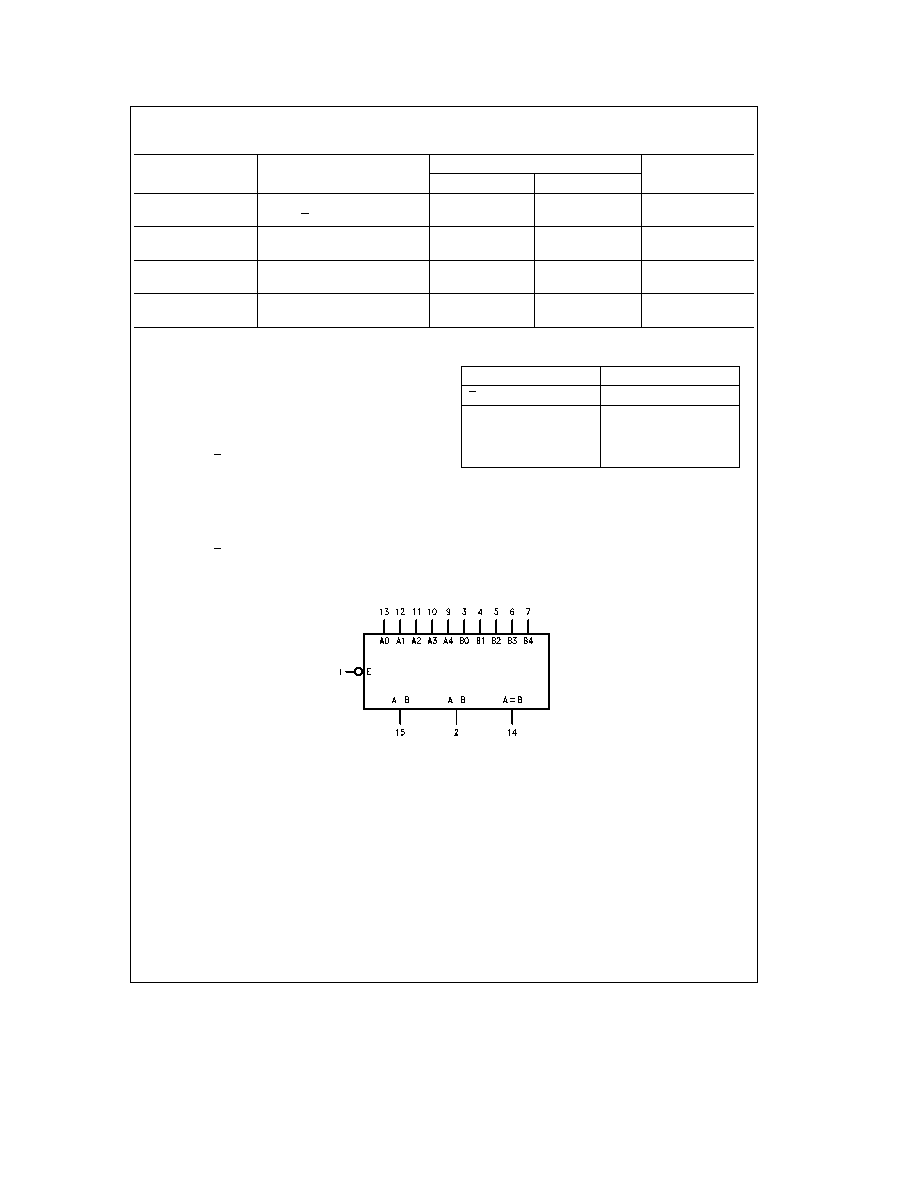
Functional Description
The '24 5-bit comparators use combinational circuitry to di-
rectly generate ``A greater than B'' and ``A less than B''
outputs As evident from the logic diagram these outputs
are generated in only three gate delays The ``A equals B''
output is generated in one additional gate delay by decoding
the ``A neither less than nor greater than B'' condition with a
NOR gate All three outputs are activated by the active LOW
Enable Input (E)
Tying the A
l
B output from one device into an A input on
another device and the A
k
B output into the corresponding
B input permits easy expansion
The A4 and B4 inputs are the most significant inputs and
A0 B0 the least significant Thus if A4 is HIGH and B4 is
LOW the A
l
B output will be HIGH regardless of all other
inputs except E
Truth Table
Inputs
Outputs
E
A
n
B
n
A
k
B
A
l
B
A
e
B
H
X
X
L
L
L
L
Word A
e
Word B
L
L
H
L
Word A
l
Word B
L
H
L
L
Word B
l
Word A
H
L
L
H
e
HIGH Voltage Level
L
e
LOW Voltage Level
X
e
Immaterial
Logic Symbol
TL F 9792 ≠ 2
V
CC
e
Pin 16
GND
e
Pin 6
3
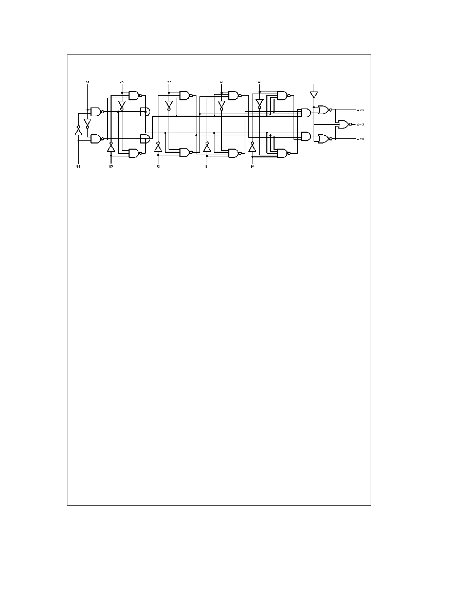
Logic Diagram
TL F 9792 ≠ 3
4

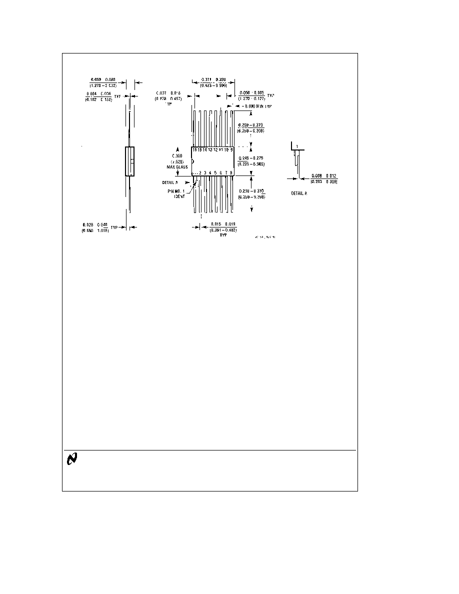
Physical Dimensions
inches (millimeters)
16-Lead Ceramic Dual-In-Line Package (J)
Order Number 9324DMQB
NS Package Number J16A
16-Lead Molded Dual-In-Line Package (N)
Order Number DM9324N
NS Package Number N16E
5
9324DM9324
5-Bit
Comparator
Physical Dimensions
inches (millimeters) (Continued)
16-Lead Ceramic Flat Package (W)
Order Number 9324FMQB
NS Package Number W16A
LIFE SUPPORT POLICY
NATIONAL'S PRODUCTS ARE NOT AUTHORIZED FOR USE AS CRITICAL COMPONENTS IN LIFE SUPPORT
DEVICES OR SYSTEMS WITHOUT THE EXPRESS WRITTEN APPROVAL OF THE PRESIDENT OF NATIONAL
SEMICONDUCTOR CORPORATION As used herein
1 Life support devices or systems are devices or
2 A critical component is any component of a life
systems which (a) are intended for surgical implant
support device or system whose failure to perform can
into the body or (b) support or sustain life and whose
be reasonably expected to cause the failure of the life
failure to perform when properly used in accordance
support device or system or to affect its safety or
with instructions for use provided in the labeling can
effectiveness
be reasonably expected to result in a significant injury
to the user
National Semiconductor
National Semiconductor
National Semiconductor
National Semiconductor
Corporation
Europe
Hong Kong Ltd
Japan Ltd
1111 West Bardin Road
Fax (a49) 0-180-530 85 86
13th Floor Straight Block
Tel 81-043-299-2309
Arlington TX 76017
Email cnjwge tevm2 nsc com
Ocean Centre 5 Canton Rd
Fax 81-043-299-2408
Tel 1(800) 272-9959
Deutsch Tel (a49) 0-180-530 85 85
Tsimshatsui Kowloon
Fax 1(800) 737-7018
English
Tel (a49) 0-180-532 78 32
Hong Kong
Fran ais Tel (a49) 0-180-532 93 58
Tel (852) 2737-1600
Italiano
Tel (a49) 0-180-534 16 80
Fax (852) 2736-9960
National does not assume any responsibility for use of any circuitry described no circuit patent licenses are implied and National reserves the right at any time without notice to change said circuitry and specifications