TL F 6609
9334DM9334
8-Bit
Addressable
Latch
June 1989
9334 DM9334 8-Bit Addressable Latch
General Description
The DM9334 is a high speed 8-bit Addressable Latch de-
signed for general purpose storage applications in digital
systems It is a multifunctional device capable of storing sin-
gle line data in eight addressable latches and being a one-
of-eight decoder and demultiplexer with active level high
outputs The device also incorporates an active level low
common clear for resetting all latches as well as an active
level low enable
The DM9334 has four modes of operation which are shown
in the mode selection table In the addressable latch mode
data on the data line (D) is written into the addressed latch
The addressed latch will follow the data input with all non-
addressed latches remaining in their previous states In the
memory mode all latches remain in their previous state and
are unaffected by the data or address inputs
In the one-of-eight decoding or demultiplexing mode the
addressed output will follow the state of the D input with all
other inputs in the low state In the clear mode all outputs
are low and unaffected by the address and data inputs
When operating the device as an addressable latch chang-
ing more than one bit of the address could impose a tran-
sient wrong address Therefore this should only be done
while in the memory mode
The function tables summarize the operation of the product
Features
Y
Common clear
Y
Easily expandable
Y
Random (addressable) data entry
Y
Serial to parallel capability
Y
8 bits of storage output of each bit available
Y
Active high demultiplexing decoding capability
Y
Alternate Military Aerospace device (9334) is available
Contact a National Semiconductor Sales Office Distrib-
utor for specifications
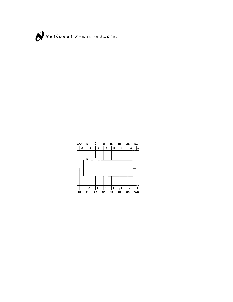
Connection Diagram
Dual-In-Line Package
TL F 6609 � 1
Order Number 9334DMQB 9334FMQB DM9334J or DM9334N
See NS Package Number J16A N16E or W16A
C1995 National Semiconductor Corporation
RRD-B30M105 Printed in U S A
Absolute Maximum Ratings
(Note)
If Military Aerospace specified devices are required
please contact the National Semiconductor Sales
Office Distributors for availability and specifications
Supply Voltage
7V
Input Voltage
5 5V
Operating Free Air Temperature Range
Military
b
55 C to
a
125 C
Commercial
0 to
a
70 C
Storage Temperature Range
b
65 C to
a
150 C
Note
The ``Absolute Maximum Ratings'' are those values
beyond which the safety of the device cannot be guaran-
teed The device should not be operated at these limits The
parametric values defined in the ``Electrical Characteristics''
table are not guaranteed at the absolute maximum ratings
The ``Recommended Operating Conditions'' table will define
the conditions for actual device operation
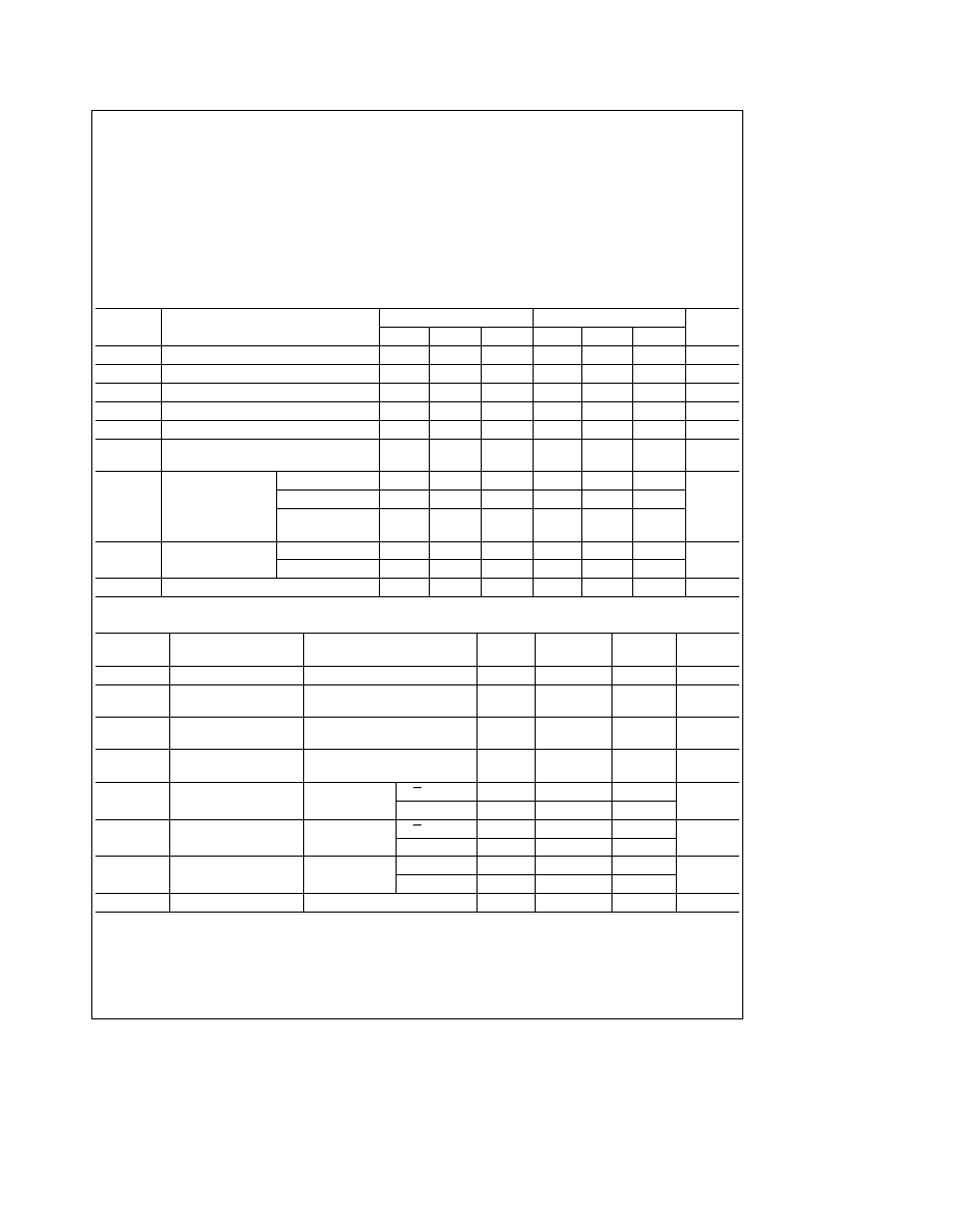
Recommended Operating Conditions
Symbol
Parameter
Military
Commercial
Units
Min
Nom
Max
Min
Nom
Max
V
CC
Supply Voltage
4 5
5
5 5
4 75
5
5 25
V
V
IH
High Level Input Voltage
2
2
V
V
IL
Low Level Input Voltage
0 8
0 8
V
I
OH
High Level Output Current
b
0 8
b
0 8
mA
I
OL
Low Level Output Current
16
16
mA
t
W
ENABLE Pulse Width
19
13
19
13
ns
(Fig 1) (Note 4)
t
SU
Setup Time
Data 1 (Fig 4)
20
13
20
13
(Note 4)
Data 0 (Fig 4)
20
14
20
14
ns
Address (Fig 6)
10
5
10
5
(Note 1)
t
H
Hold Time
Data 1 (Fig 4)
0
b
10
0
b
10
ns
(Note 4)
Data 0 (Fig 4)
0
b
13
0
b
13
T
A
Free Air Operating Temperature
b
55
125
0
70
C
Electrical Characteristics
over recommended operating free air temperature range (unless otherwise noted)
Symbol
Parameter
Conditions
Min
Typ
Max
Units
(Note 2)
V
I
Input Clamp Voltage
V
CC
e
Min I
I
e b
12 mA
b
1 5
V
V
OH
High Level Output
V
CC
e
Min I
OH
e
Max
2 4
3 6
V
Voltage
V
IL
e
Max V
IH
e
Min
V
OL
Low Level Output
V
CC
e
Min I
OL
e
Max
0 2
0 4
V
Voltage
V
IH
e
Min V
IL
e
Max
I
I
Input Current
Max
V
CC
e
Max V
I
e
5 5V
1
mA
Input Voltage
I
IH
High Level Input
V
CC
e
Max
E Input
60
m
A
Current
V
I
e
2 4V
Others
40
I
IL
Low Level Input
V
CC
e
Max
E Input
b
2 4
mA
Current
V
I
e
0 4V
Others
b
1 6
I
OS
Short Circuit
V
CC
e
Max
MIL
b
30
b
100
mA
Output Current
(Note 3)
COM
b
30
b
100
I
CC
Supply Current
V
CC
e
Max
56
86
mA
Note 1
The ADDRESS setup time is the time before the negative ENABLE transition that the ADDRESS must be stable so that the correct latch is addressed
without affecting the other latches
Note 2
All typicals are at V
CC
e
5V T
A
e
25 C
Note 3
Not more than one output should be shorted at a time and the duration should not exceed one second
Note 4
T
A
e
25 C and V
CC
e
5V
2

Switching Characteristics
at V
CC
e
5V and T
A
e
25 C (See Section 1 for Test Waveforms and Output Load)
Symbol
Parameter
From (Input)
R
L
e
400X C
L
e
15 pF
Units
To (Output)
Min
Max
t
PLH
Propagation Delay Time
Enable to
28
ns
Low to High Level Output
Output Fig 1
t
PHL
Propagation Delay Time
Enable to
27
ns
High to Low Level Output
Output Fig 1
t
PLH
Propagation Delay Time
Data to
35
ns
Low to High Level Output
Output Fig 2
t
PHL
Propagation Delay Time
Data to
28
ns
High to Low Level Output
Output Fig 2
t
PLH
Propagation Delay Time
Address to
35
ns
Low to High Level Output
Output Fig 3
t
PHL
Propagation Delay Time
Address to
35
ns
High to Low Level Output
Output Fig 3
t
PHL
Propagation Delay Time
Clear to
31
ns
High to Low Level Output
Output Fig 5
Function Tables
E
C
Mode
L
H
Addressable Latch
H
H
Memory
L
L
Active High Eight
Channel Demultiplexer
H
L
Clear
Inputs
Present Output States
Mode
C
E
D
A0
A1
A2
Q0
Q1
Q2
Q3
Q4
Q5
Q6
Q7
L
H
X
X
X
X
L
L
L
L
L
L
L
L
Clear
L
L
L
L
L
L
L
L
L
L
L
L
L
L
L
L
H
L
L
L
H
L
L
L
L
L
L
L
L
L
L
H
L
L
L
L
L
L
L
L
L
L
L
L
H
H
L
L
L
H
L
L
L
L
L
L
Demultiplex
L
L
H
H
H
H
L
L
L
L
L
L
L
H
H
H
X
X
X
X
Q
Nb1
Memory
H
L
L
L
L
L
L
Q
Nb1
Q
Nb1
Q
Nb1
H
L
H
L
L
L
H
Q
Nb1
Q
Nb1
H
L
L
H
L
L
Q
Nb1
L
Q
Nb1
H
L
H
H
L
L
Q
Nb1
H
Q
Nb1
Addressable
Latch
H
L
L
H
H
H
Q
Nb1
Q
Nb1
L
H
L
H
H
H
H
Q
Nb1
Q
Nb1
H
X
e
Don't Care Condition
L
e
Low Voltage Level
H
e
High Voltage Level
Q
N
b
1
e
Previous Output State
3

Logic Diagram
9334
TL F 6609 � 2
Switching Time Waveforms
TL F 6609 � 3
Other Conditions C
e
H A
e
Stable
Figure 1
TL F 6609 � 4
Other Conditions E
e
L C
e
H A
e
Stable
Figure 2
TL F 6609 � 5
Other Conditions E
e
L C
e
L D
e
H
Figure 3
TL F 6609 � 6
Other Conditions C
e
H A
e
Stable
Figure 4
TL F 6609 � 7
Other Conditons E
e
H
Figure 5
TL F 6609 � 8
Other Conditions C
e
H
Figure 6
Note
The shaded areas indicate when the inputs are permitted to change for predictable output performance
4

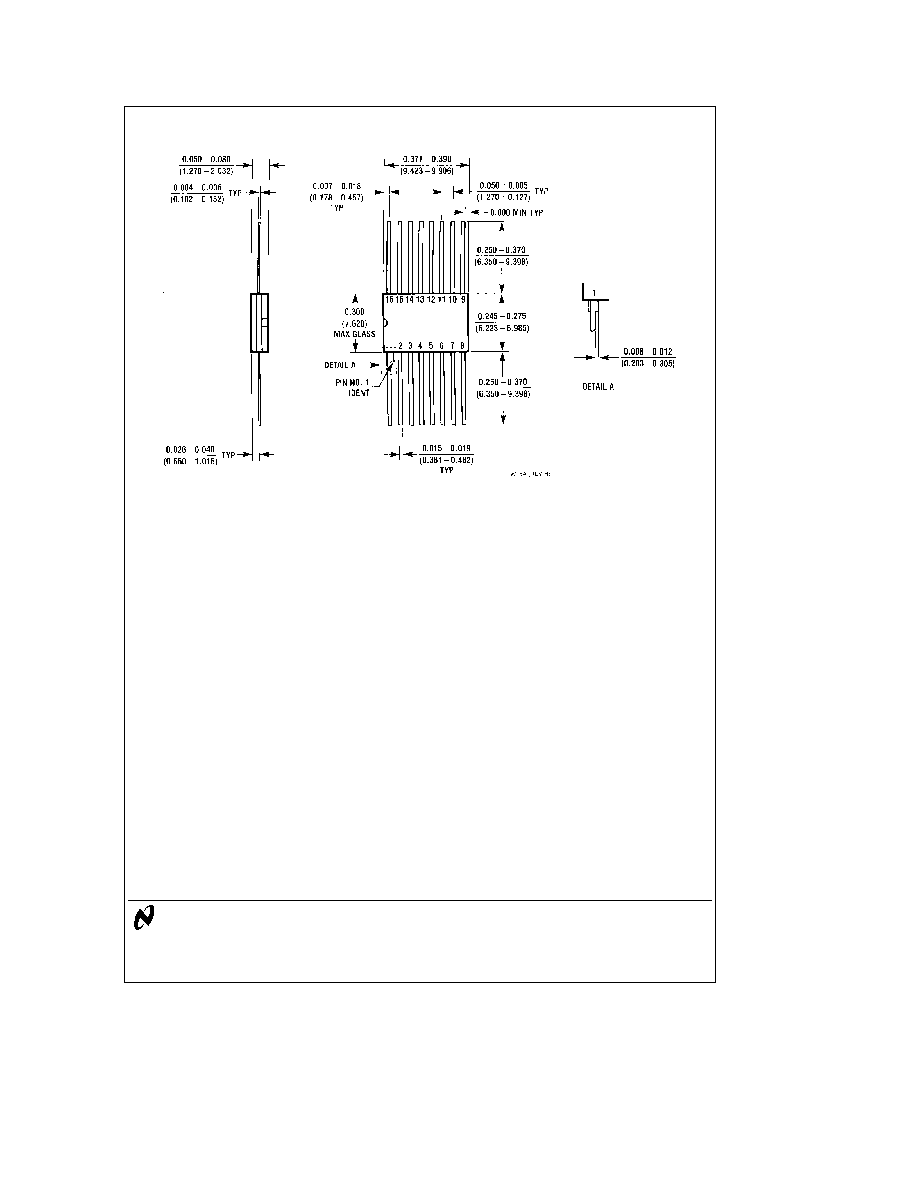
Physical Dimensions
inches (millimeters)
16-Lead Ceramic Dual-In-Line Package (J)
Order Number 9334DMQB or DM9334J
NS Package Number J16A
16-Lead Molded Dual-In-Line Package (N)
Order Number DM9334N
NS Package Number N16E
5
9334DM9334
8-Bit
Addressable
Latch
Physical Dimensions
inches (millimeters) (Continued)
16-Lead Ceramic Flat Package (W)
Order Number 9334FMQB
NS Package Number W16A
LIFE SUPPORT POLICY
NATIONAL'S PRODUCTS ARE NOT AUTHORIZED FOR USE AS CRITICAL COMPONENTS IN LIFE SUPPORT
DEVICES OR SYSTEMS WITHOUT THE EXPRESS WRITTEN APPROVAL OF THE PRESIDENT OF NATIONAL
SEMICONDUCTOR CORPORATION As used herein
1 Life support devices or systems are devices or
2 A critical component is any component of a life
systems which (a) are intended for surgical implant
support device or system whose failure to perform can
into the body or (b) support or sustain life and whose
be reasonably expected to cause the failure of the life
failure to perform when properly used in accordance
support device or system or to affect its safety or
with instructions for use provided in the labeling can
effectiveness
be reasonably expected to result in a significant injury
to the user
National Semiconductor
National Semiconductor
National Semiconductor
National Semiconductor
Corporation
Europe
Hong Kong Ltd
Japan Ltd
1111 West Bardin Road
Fax (a49) 0-180-530 85 86
13th Floor Straight Block
Tel 81-043-299-2309
Arlington TX 76017
Email cnjwge tevm2 nsc com
Ocean Centre 5 Canton Rd
Fax 81-043-299-2408
Tel 1(800) 272-9959
Deutsch Tel (a49) 0-180-530 85 85
Tsimshatsui Kowloon
Fax 1(800) 737-7018
English
Tel (a49) 0-180-532 78 32
Hong Kong
Fran ais Tel (a49) 0-180-532 93 58
Tel (852) 2737-1600
Italiano
Tel (a49) 0-180-534 16 80
Fax (852) 2736-9960
National does not assume any responsibility for use of any circuitry described no circuit patent licenses are implied and National reserves the right at any time without notice to change said circuitry and specifications