
TL H 5670
ADC0800
8-Bit
AD
Converter
February 1995
ADC0800 8-Bit A D Converter
General Description
The ADC0800 is an 8-bit monolithic A D converter using P-
channel ion-implanted MOS technology It contains a high
input impedance comparator 256 series resistors and ana-
log switches control logic and output latches Conversion is
performed using a successive approximation technique
where the unknown analog voltage is compared to the re-
sistor tie points using analog switches When the appropri-
ate tie point voltage matches the unknown voltage conver-
sion is complete and the digital outputs contain an 8-bit
complementary binary word corresponding to the unknown
The binary output is TRI-STATE
to permit bussing on com-
mon data lines
The ADC0800PD is specified over
b
55 C to
a
125 C and
the ADC0800PCD is specified over 0 C to 70 C
Features
Y
Low cost
Y
g
5V 10V input ranges
Y
No missing codes
Y
Ratiometric conversion
Y
TRI-STATE outputs
Y
Fast
T
C
e
50 ms
Y
Contains output latches
Y
TTL compatible
Y
Supply voltages
5 V
DC
and
b
12 V
DC
Y
Resolution
8 bits
Y
Linearity
g
1 LSB
Y
Conversion speed
40 clock periods
Y
Clock range
50 to 800 kHz
Block Diagram
TL H 5670 ≠ 1
(00000000
e a
full-scale)
TRI-STATE
is a registered trademark of National Semiconductor Corp
C1995 National Semiconductor Corporation
RRD-B30M115 Printed in U S A
Absolute Maximum Ratings
(Note 1)
If Military Aerospace specified devices are required
please contact the National Semiconductor Sales
Office Distributors for availability and specifications
Supply Voltage (V
DD
)
V
SS
b
22V
Supply Voltage (V
GG
)
V
SS
b
22V
Voltage at Any Input
V
SS
a
0 3V to V
SS
b
22V
Input Current at Any Pin (Note 2)
5 mA
Package Input Current (Note 2)
20 mA
Power Dissipation (Note 3)
875 mW
ESD Susceptibility (Note 4)
500V
Storage Temperature
150 C
Lead Temperature (Soldering 10 sec )
300 C
Operating Ratings
(Note 1)
Temperature Range
T
MIN
s
T
A
s
T
MAX
ADC0800PD
b
55 C
s
T
A
s
a
125 C
ADC0800PCD
0 C
s
T
A
s
a
70 C
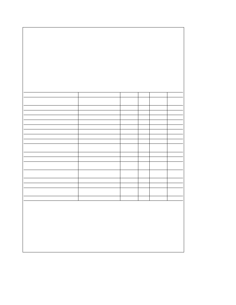
Electrical Characteristics
These specifications apply for V
SS
e
5 0 V
DC
V
GG
e b
12 0 V
DC
V
DD
e
0 V
DC
a reference voltage of 10 000 V
DC
across the
on-chip R-network (V
R-NETWORK TOP
e
5 000 V
DC
and V
R-NETWORK BOTTOM
e b
5 000 V
DC
) and a clock frequency of 800
kHz For all tests a 475X resistor is used from pin 5 to V
R-NETWORK BOTTOM
e
b
5 V
DC
Unless otherwise noted these
specifications apply over an ambient temperature range of
b
55 C to
a
125 C for the ADC0800PD and 0 C to
a
70 C for the
ADC0800PCD
Parameter
Conditions
Min
Typ
Max
Units
Non-Linearity
T
A
e
25 C (Note 8)
g
1
LSB
Over Temperature (Note 8)
g
2
LSB
Differential Non-Linearity
g
LSB
Zero Error
g
2
LSB
Zero Error Temperature Coefficient
(Note 9)
0 01
% C
Full-Scale Error
g
2
LSB
Full-Scale Error Temperature Coefficient
(Note 9)
0 01
% C
Input Leakage
1
m
A
Logical ``1'' Input Voltage
All Inputs
V
SS
b
1 0
V
SS
V
Logical ``0'' Input Voltage
All Inputs
V
GG
V
SS
b
4 2
V
Logical Input Leakage
T
A
e
25 C All Inputs V
IL
e
1
m
A
V
SS
b
10V
Logical ``1'' Output Voltage
All Outputs I
OH
e
100 mA
2 4
V
Logical ``0'' Output Voltage
All Outputs I
OL
e
1 6 mA
0 4
V
Disabled Output Leakage
T
A
e
25 C All Outputs V
OL
e
2
m
A
V
SS
10V
Clock Frequency
0 C
s
T
A
s
a
70 C
50
800
kHz
b
55 C
s
T
A
s
a
125 C
100
500
kHz
Clock Pulse Duty Cycle
40
60
%
TRI-STATE Enable Disable Time
1
m
s
Start Conversion Pulse
(Note 10)
1
3
Clock
Periods
Power Supply Current
T
A
e
25 C
20
mA
Note 1
Absolute Maximum Ratings indicate limits beyond which damage to the device may occur DC and AC electrical specifications do not apply when operating
the device beyond its specified operating conditions
Note 2
When the input voltage (V
IN
) at any pin exceeds the power supply rails (V
IN
k
V
b
or V
IN
l
V
a
) the absolute value of current at that pin should be limited
to 5 mA or less The 20 mA package input current limits the number of pins that can exceed the power supply boundaries with a 5 mA current limit to four
Note 3
The maximum power dissipation must be derated at elevated temperatures and is dictated by T
JMAX
i
JA
and the ambient temperature T
A
The maximum
allowable power dissipation at any temperature is P
D
e
(T
JMAX
b
T
A
) i
JA
or the number given in the Absolute Maximum Ratings whichever is lower For this
device T
JMAX
e
125 C and the typical junction-to-ambient thermal resistance of the ADC0800PD and ADC0800PCD when board mounted is 66 C W
Note 4
Human body model 100 pF discharged through a 1 5 kX resistor
Note 5
Typicals are at 25 C and represent most likely parametric norm
Note 6
Tested limits are guaranteed to National's AOQL (Average Outgoing Quality Level)
Note 7
Design limits are guaranteed but not 100% tested These limits are not used to calculate outgoing quality levels
Note 8
Non-linearity specifications are based on best straight line
Note 9
Guaranteed by design only
Note 10
Start conversion pulse duration greater than 3
clock periods will cause conversion errors
2
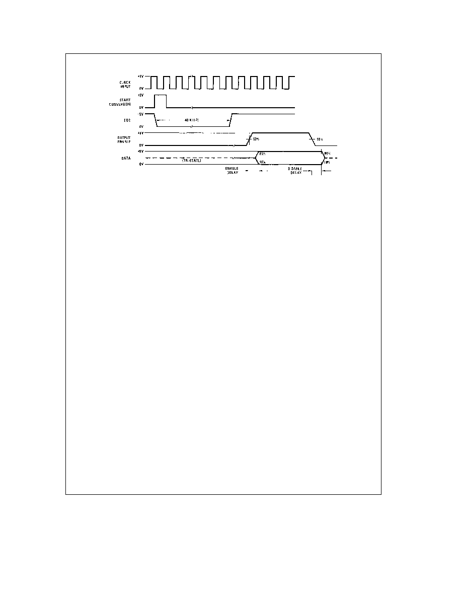
Timing Diagram
TL H 5670 ≠ 2
Data is complementary binary (full scale is all ``0's'' output)
Application Hints
OPERATION
The ADC0800 contains a network with 256-300X resistors
in series Analog switch taps are made at the junction of
each resistor and at each end of the network In operation
a reference (10 00V) is applied across this network of 256
resistors An analog input (V
IN
) is first compared to the cen-
ter point of the ladder via the appropriate switch If V
IN
is
larger than V
REF
2 the internal logic changes the switch
points and now compares V
IN
and
V
REF
This process
known as successive approximation continues until the
best match of V
IN
and V
REF
N is made N now defines a
specific tap on the resistor network When the conversion is
complete the logic loads a binary word corresponding to
this tap into the output latch and an end of conversion
(EOC) logic level appears The output latches hold this data
valid until a new conversion is completed and new data is
loaded into the latches The data transfer occurs in about
200 ns so that valid data is present virtually all the time in
the latches The data outputs are activated when the Output
Enable is high and in TRI-STATE when Output Enable is
low The Enable Delay time is approximately 200 ns Each
conversion requires 40 clock periods The device may be
operated in the free running mode by connecting the Start
Conversion line to the End of Conversion line However to
ensure start-up under all possible conditions an external
Start Conversion pulse is required during power up condi-
tions
REFERENCE
The reference applied across the 256 resistor network de-
termines the analog input range V
REF
e
10 00V with the top
of the R-network connected to 5V and the bottom connect-
ed to
b
5V gives a
g
5V range The reference can be level
shifted between V
SS
and V
GG
However the voltage ap-
plied to the top of the R-network (pin 15) must not exceed
V
SS
to prevent forward biasing the on-chip parasitic silicon
diodes that exist between the P-diffused resistors (pin 15)
and the N-type body (pin 10 V
SS
) Use of a standard logic
power supply for V
SS
can cause problems both due to initial
voltage tolerance and changes over temperature A solution
is to power the V
SS
line (15 mA max drain) from the output
of the op amp that is used to bias the top of the
R-network (pin 15) The analog input voltage and the volt-
age that is applied to the bottom of the R-network (pin 5)
must be at least 7V above the
b
V
GG
supply voltage to
ensure adequate voltage drive to the analog switches
Other reference voltages may be used (such as 10 24V) If a
5V reference is used the analog range will be 5V and accu-
racy will be reduced by a factor of 2 Thus for maximum
accuracy it is desirable to operate with at least a 10V refer-
ence For TTL logic levels this requires 5V and
b
5V for the
R-network CMOS can operate at the 10 V
DC
V
SS
level and
a single 10 V
DC
reference can be used All digital voltage
levels for both inputs and outputs will be from ground to
V
SS
ANALOG INPUT AND SOURCE RESISTANCE
CONSIDERATIONS
The lead to the analog input (pin 12) should be kept as short
as possible Both noise and digital clock coupling to this
input can cause conversion errors To minimize any input
errors
the following source resistance considerations
should be noted
For R
S
s
5k
No analog input bypass capacitor re-
quired although a 0 1 mF input bypass
capacitor will prevent pickup due to un-
avoidable series lead inductance
For 5k
k
R
S
s
20k
A 0 1 mF capacitor from the input (pin
12) to ground should be used
For R
S
l
20k
Input buffering is necessary
If the overall converter system requires lowpass filtering of
the analog input signal use a 20 kX or less series resistor
for a passive RC section or add an op amp RC active low-
pass filter (with its inherent low output resistance) to ensure
accurate conversions
CLOCK COUPLING
The clock lead should be kept away from the analog input
line to reduce coupling
LOGIC INPUTS
The logical ``1'' input voltage swing for the Clock Start Con-
version and Output Enable should be (V
SS
b
1 0V)
3
Application Hints
(Continued)
CMOS will satisfy this requirement but a pull-up resistor
should be used for TTL logic inputs
RE-START AND DATA VALID AFTER EOC
The EOC line (pin 9) will be in the low state for a maximum
of 40 clock periods to indicate ``busy'' A START pulse that
occurs while the A D is BUSY will reset the SAR and start a
new conversion with the EOC signal remaining in the low
state until the end of this new conversion When the conver-
sion is complete the EOC line will go to the high voltage
state An additional 4 clock periods must be allowed to
elapse after EOC goes high before a new conversion cycle
is requested Start Conversion pulses that occur during this
last 4 clock period interval may be ignored (see
Figure 1 and
2 for high speed operation) This is a problem only for high
conversion rates and keeping the number of conversions
per second less than f
CLOCK
44 automatically guarantees
proper operation For example for an 800 kHz clock ap-
proximately 18 000 conversions per second are allowed
The transfer of the new digital data to the output is initiated
when EOC goes to the high voltage state
POWER SUPPLIES
Standard supplies are V
SS
e a
5V
V
GG
e b
12V and
V
DD
e
0V Device accuracy is dependent on stability of the
reference voltage and has slight sensitivity to V
SS
V
GG
V
DD
has no effect on accuracy Noise spikes on the V
SS
and V
GG
supplies can cause improper conversion there-
fore filtering each supply with a 4 7 mF tantalum capacitor is
recommended
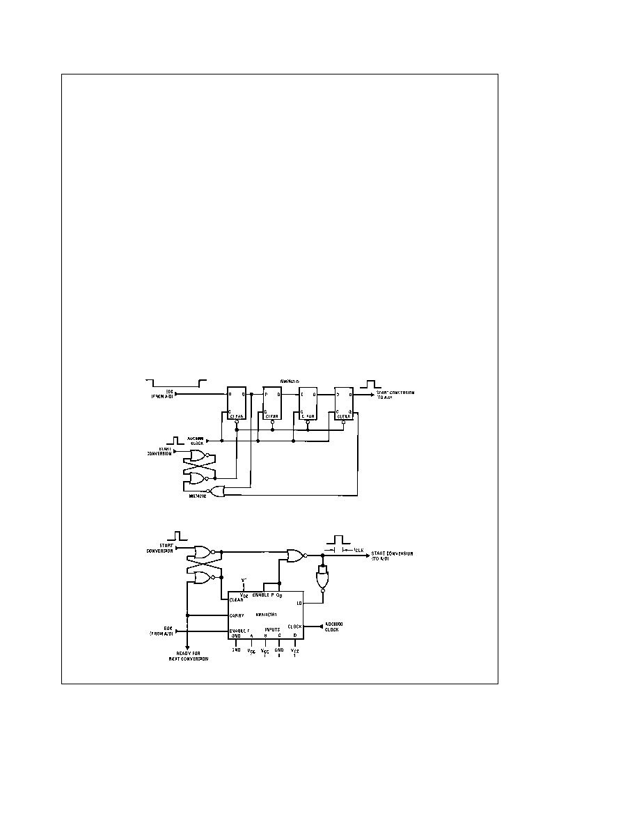
CONTINUOUS CONVERSIONS AND LOGIC CONTROL
Simply tying the EOC output to the Start Conversion input
will allow continuous conversions but an oscillation on this
line will exist during the first 4 clock periods after EOC goes
high Adding a D flip-flop between EOC (D input) to Start
Conversion (Q output) will prevent the oscillation and will
allow a stop continuous control via the ``clear'' input
To prevent missing a start pulse that may occur after EOC
goes high and prior to the required 4 clock period time inter-
val the circuit of
Figure 1 can be used The RS latch can be
set at any time and the 4-stage shift register delays the
application of the start pulse to the A D by 4 clock periods
The RS latch is reset 1 clock period after the A D EOC
signal goes to the low voltage state This circuit also pro-
vides a Start Conversion pulse to the A D which is 1 clock
period wide
A second control logic application circuit is shown in
Figure
2
This allows an asynchronous start pulse of arbitrary
length less than T
C
to continuously convert for a fixed high
level and provides a single clock period start pulse to the
A D The binary counter is loaded with a count of 11 when
the start pulse to the A D appears Counting is inhibited
until the EOC signal from the A D goes high A carry pulse
is then generated 4 clock periods after EOC goes high and
is used to reset the input RS latch This carry pulse can be
used to indicate that the conversion is complete the data
has transferred to the output buffers and the system is
ready for a new conversion cycle
TL H 5670 ≠ 3
FIGURE 1 Delaying an Asynchronous Start Pulse
TL H 5670 ≠ 10
FIGURE 2 A D Control Logic
4
Application Hints
(Continued)
ZERO AND FULL-SCALE ADJUSTMENT
Zero Adjustment
This is the offset voltage required at the
bottom of the R-network (pin 5) to make the 11111111 to
11111110 transition when the input voltage is
LSB (20
mV for a 10 24V scale) In most cases this can be accom-
plished by having a 1 kX pot on pin 5 A resistor of 475X
can be used as a non-adjustable best approximation from
pin 5 to ground
Full-Scale Adjustment
This is the offset voltage required
at the top of the R-network (pin 15) to make the 00000001
to 00000000 transition when the input voltage is 1
LSB
from full-scale (60 mV less than full-scale for a 10 24V
scale) This voltage is guaranteed to be within
g
2 LSB for
the ADC0800 without adjustment In most cases adjust-
ment can be accomplished by having a 1 kX pot on pin 15
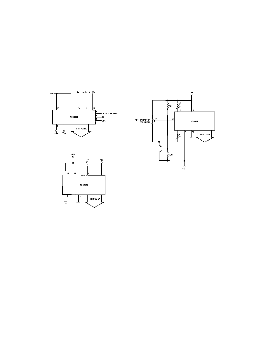
Typical Applications
General Connection
TL H 5670 ≠ 11
Hi-Voltage CMOS Output Levels
0V to 10V V
IN
range
0V to 10V output levels
TL H 5670 ≠ 12
Ratiometric Input Signal with Tracking Reference
TL H 5670 ≠ 4
5